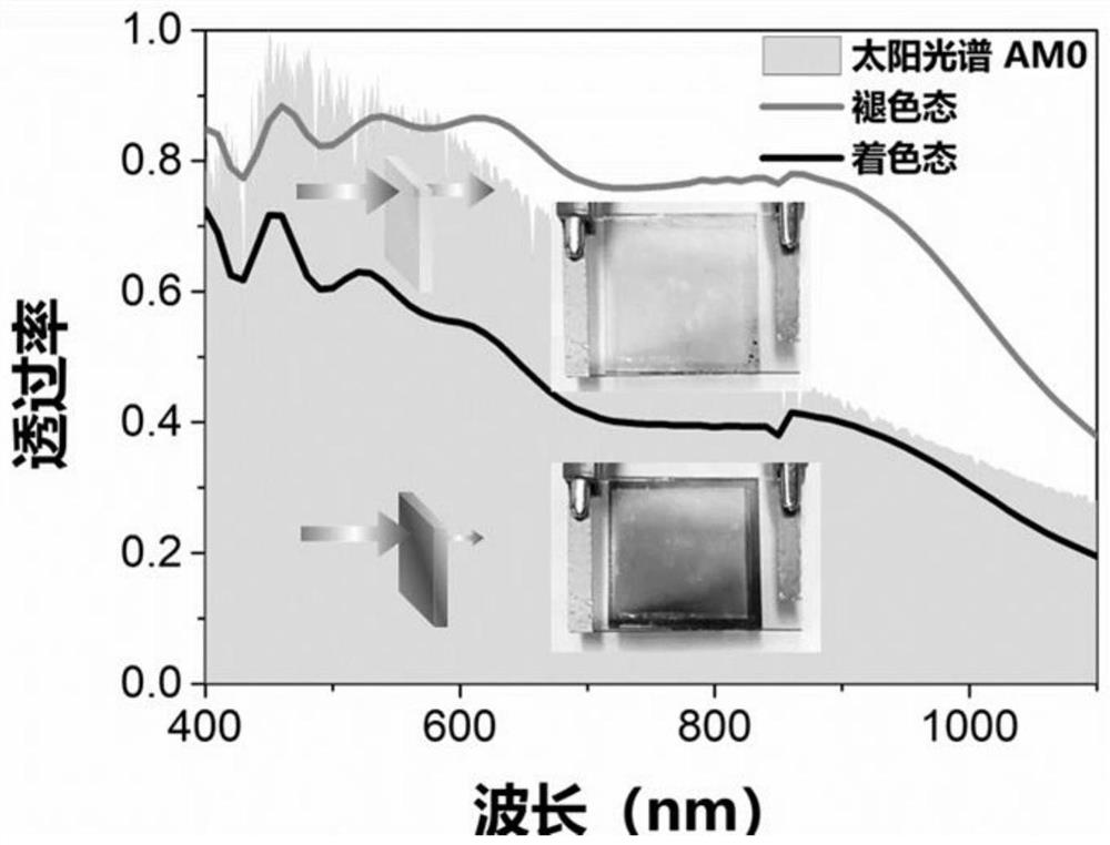
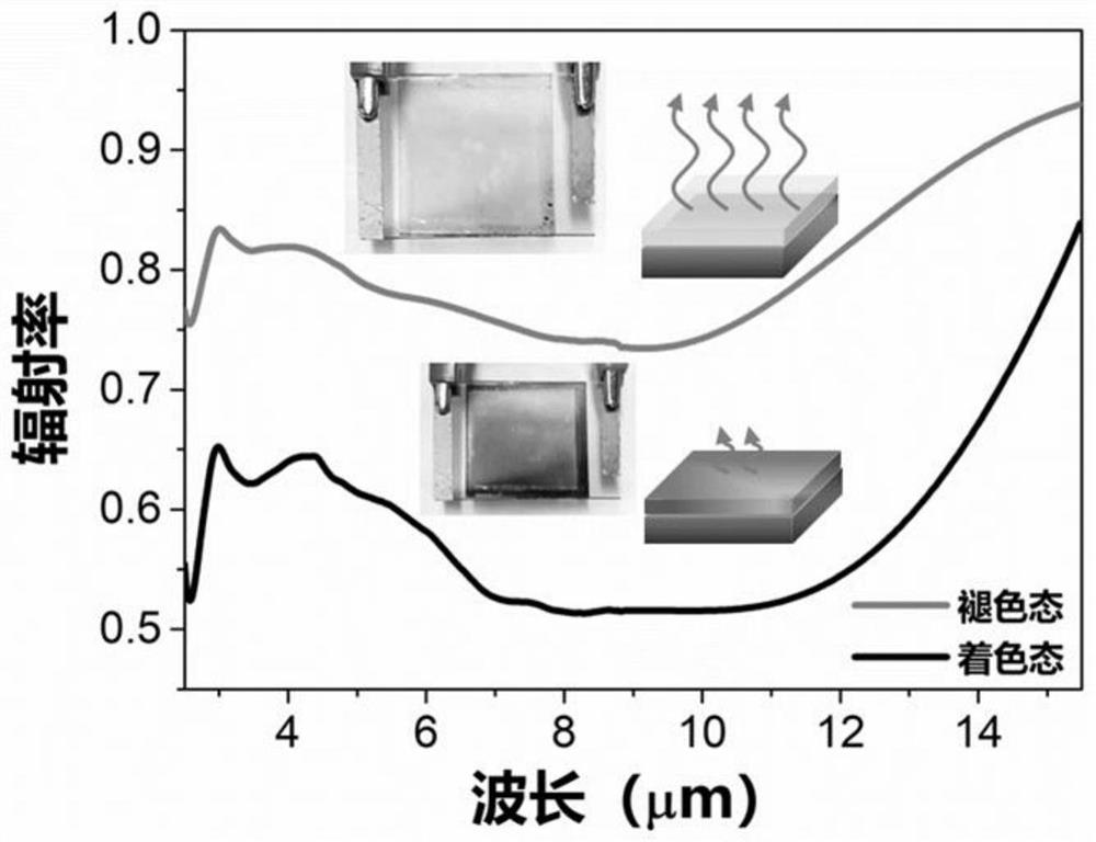
Visible to mid-infrared band electrochromic thin film device with adjustable light performance and preparation method
A technology of electrochromic and thin-film devices, which is applied in the direction of originals for photomechanical processing, photographic process of patterned surfaces, and instruments. Control performance, reduce the effect of reflection
- Summary
- Abstract
- Description
- Claims
- Application Information
AI Technical Summary
Problems solved by technology
Method used
Image
Examples
preparation example Construction
[0040] A method for preparing an electrochromic thin film device with adjustable light performance in the visible to mid-infrared band, comprising the following steps:
[0041] S1: Select the substrate, the material of the substrate is a visible or infrared highly transparent inorganic material, such as: CaF 2 , BaF 2 , NaCl, KBr, etc. (0.3-25μm transmittance greater than 92%), or highly transparent inorganic materials for the required band, such as SiO 2 or ITO glass; and pre-treat the substrate;
[0042] The specific process of pretreatment can be determined according to specific materials, for example:
[0043] For deliquescent salt windows such as NaCl and KBr, the pre-treatment is preferably polishing and drying. The whole pre-treatment process needs to avoid the material from being damp and reducing its transmittance;
[0044] For corrosion-resistant windows such as silicon dioxide and conductive glass that are not easy to deliquesce, it is preferable to perform regul...
Embodiment 1
[0064] S1: Select high-temperature-resistant quartz glass (silicon dioxide sheet) with a thickness less than or equal to 1 mm and an area of less than 6 inches as the base material; ultrasonically clean the silicon dioxide sheet in toluene for 20 minutes, and ultrasonically clean it in acetone for 15 minutes. Ultrasonic cleaning in ethanol for 20 minutes, and finally ultrasonic cleaning in deionized water for 20 minutes, rinse several times with flowing deionized water, and dry;
[0065] S2: The treated silicon dioxide wafer is subjected to plasma surface treatment for 10 minutes, and then electron beam evaporation is used to deposit 10nm of chromium and 60nm of gold successively. The role of chromium is to enhance the adhesion of the deposit on the glass sheet; Spin-coat positive photoresist with a thickness of 3 microns on the top, cover a mask plate with a grid array with a side width of 100 microns and a line width of 5 microns, and perform 10 seconds of UV exposure and 1...
Embodiment 2
[0071] S1: Select ITO conductive glass with a thickness less than or equal to 1 mm and an area less than 6 inches as the base material, and perform pretreatment on the ITO glass as in the ultrasonic cleaning step in step S1 of the above-mentioned embodiment 1;
[0072] S2: Simultaneous magnetron sputtering deposition of 350 nm WO on two pieces of ITO glass 3 , the sputtering power is 300W, the ratio of argon to oxygen is 30:2;
[0073] S3: Re-deposit 100nm Ta on one of them 2 o 5 , the sputtering power was 300W, the ratio of argon to oxygen was 30:3, and then the Ta 2 o 5 The ITO glass was annealed in an argon atmosphere, and the temperature was raised with the furnace at a rate of 1°C / min. The temperature was raised to 550°C, kept for 3 hours, cooled with the furnace, and the sample was connected to the electrochemical workstation through a three-electrode system. The ions were taken in several times by cyclic voltammetry, and the electrolyte was lithium perchlorate / propy...
PUM
| Property | Measurement | Unit |
|---|---|---|
| thickness | aaaaa | aaaaa |
| thickness | aaaaa | aaaaa |
| thickness | aaaaa | aaaaa |
Abstract
Description
Claims
Application Information

