Vacancy perovskite material-based solar cell and preparation method thereof
A technology of solar cells and perovskite materials, applied in the fields of photoelectric conversion and solar cells, can solve problems such as toxicity, poor stability of light-absorbing layers, and affect device applications, and achieve the effects of eliminating toxicity, improving light-absorbing ability, and improving environmental protection
- Summary
- Abstract
- Description
- Claims
- Application Information
AI Technical Summary
Problems solved by technology
Method used
Image

Examples
Embodiment 1
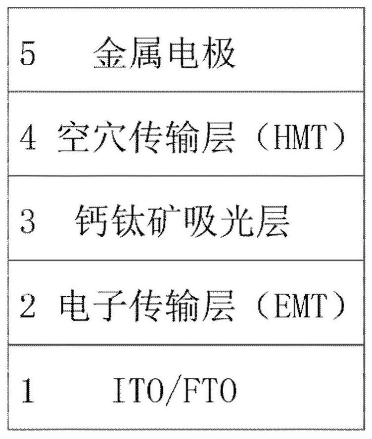
[0037] Example 1: Preparation of transparent conductive substrate using indium tin oxide ITO, electron transport layer using [6,6]-phenyl C61 Methyl butyrate PCBM, perovskite absorbing layer using Cs 2 SnI 6 , the hole transport layer uses Spiro-OMeTAD, and the top metal electrode uses silver Ag perovskite solar cells.
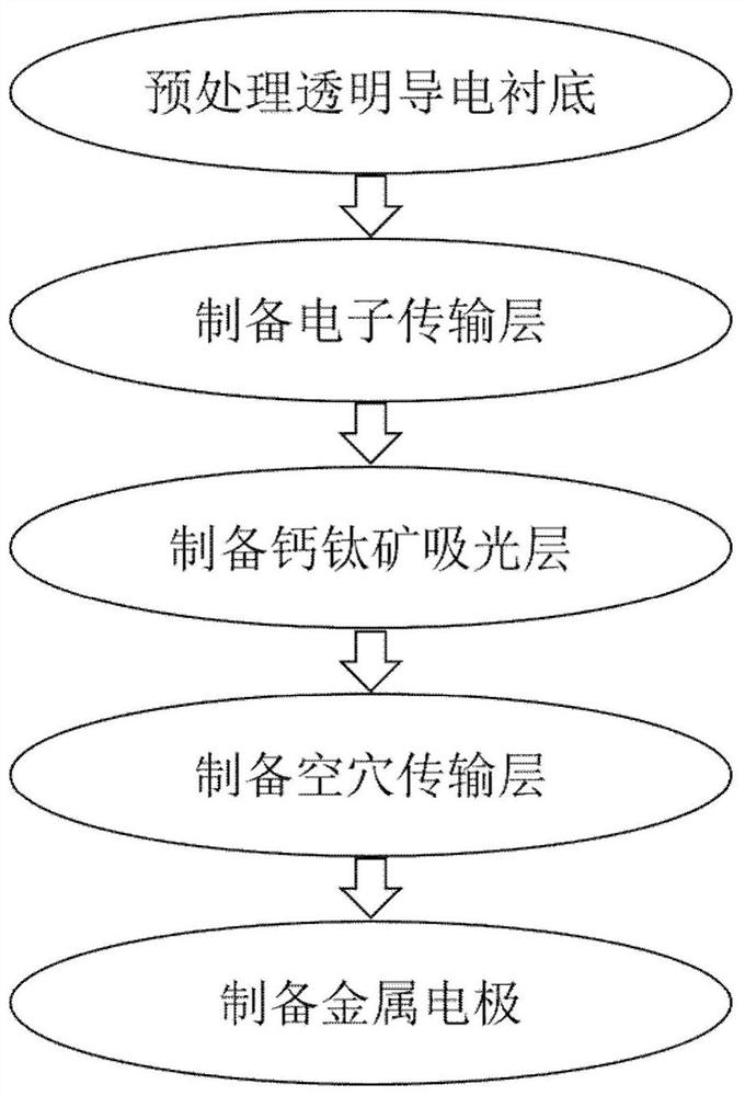
[0038] In step 1, a transparent conductive substrate is selected and pretreated.
[0039] 1.1) Select 400nm thick ITO as the transparent conductive substrate;
[0040] 1.2) Use glass cleaning solution, deionized water, acetone, isopropanol solution, and deionized water in order to clean the selected substrate ultrasonically for 20 minutes at a temperature of 50 degrees Celsius;
[0041] 1.3) Dry the glass surface of the ultrasonically cleaned substrate with nitrogen, and irradiate the glass surface with ultraviolet ozone for 20 minutes to obtain a pretreated transparent conductive substrate.
[0042] Step 2, preparing the electron transport layer of the per...
Embodiment 2
[0053] Example 2: Preparation of transparent conductive substrate using indium tin oxide ITO, electron transport layer ZnO, perovskite light absorbing layer using Cs 2 TiI 6-x Cl x A perovskite solar cell with copper thiocyanate (CuSCN) as the hole transport layer and Cu as the top metal electrode.
[0054] In step 1, select an ITO transparent conductive substrate and perform pretreatment on it.
[0055] The specific implementation of this step is the same as Step 1 of Example 1.
[0056] Step 2, preparing the electron transport layer of the perovskite solar cell.
[0057] 2.1) Add 2.95g of zinc acetate powder into 125mL of methanol solution, immediately raise the temperature to 70°C, and keep stirring to obtain transparent liquid A;
[0058] 2.2) Dissolve 1.48g of potassium hydroxide powder in 65mL of methanol solution at 70°C, and keep stirring to obtain mixed solution B;
[0059] 2.3) Add the mixed solution B dropwise to the transparent solution A while stirring, then ...
Embodiment 3
[0071] Example 3: Prepare the transparent conductive substrate using FTO, and the electron transport layer using [6,6]-phenyl C 61 Methyl butyrate PCBM, perovskite light absorbing layer using Cs 2 ZrI 6 , the hole transport layer uses poly[bis(4-phenyl)(2,4,6-trimethylphenyl)amine]PTAA, and the top metal electrode uses Au perovskite solar cells.
[0072] In step A, a transparent conductive substrate is selected and pretreated.
[0073] A1) select 400nm thick FTO as the transparent conductive substrate;
[0074] A2) Pretreat the selected substrate:
[0075] The pretreatment implementation of this step is the same as the 1.2)-1.3) step of embodiment 1.
[0076] Step B, preparing an electron transport layer.
[0077] In the glove box, 20 mg of [6,6]-phenyl C 61 Methyl butyrate PCBM was dissolved in 1mL of chlorobenzene, stirred with a magnetic stirring table for 8 hours to fully dissolve, and spin-coated with a homogenizer at a speed of 2000rpm for 45s to obtain a prepared ...
PUM
| Property | Measurement | Unit |
|---|---|---|
| thickness | aaaaa | aaaaa |
| thickness | aaaaa | aaaaa |
| thickness | aaaaa | aaaaa |
Abstract
Description
Claims
Application Information
 - R&D
- Intellectual Property
- Life Sciences
- Materials
- Tech Scout
- Unparalleled Data Quality
- Higher Quality Content
- 60% Fewer Hallucinations
Browse by: Latest US Patents, China's latest patents, Technical Efficacy Thesaurus, Application Domain, Technology Topic, Popular Technical Reports.
© 2025 PatSnap. All rights reserved.Legal|Privacy policy|Modern Slavery Act Transparency Statement|Sitemap|About US| Contact US: help@patsnap.com