
Semiconductor laser element

A technology of laser components and semiconductors, applied in the direction of semiconductor lasers, laser components, lasers, etc., can solve the problems of laser mode gain reduction, quantum well luminous efficiency, electron leakage, etc., to improve the intensity and peak gain, and improve the optical limit effect, reducing the effects of fluctuations and strains

Pending Publication Date: 2022-07-29
安徽格恩半导体有限公司
View PDF0 Cites 0 Cited by
  • Summary
  • Abstract
  • Description
  • Claims
  • Application Information

AI Technical Summary

Problems solved by technology

Nitride semiconductor lasers have the following problems: 1) Large internal lattice mismatch and large strain cause strong polarization effects, and QCSE quantum confinement Stark effect strongly limits the improvement of laser lasing gain; 2) High internal defect density and poor crystal quality Ideal; 3) The Mg acceptor activation energy of the p-type semiconductor is large, the ionization efficiency is low, the hole concentration is much lower than the electron concentration, and the hole mobility is much smaller than the electron mobility, resulting in a serious asymmetry of the electron hole in the quantum well Mismatch; 4) electron leakage; 5) low hole injection efficiency; 6) carrier delocalization; 7) strong Auger recombination; 8) high absorption loss of optical waveguide; 9) low luminous efficiency of quantum well; 10 ) p-type resistance and poor ohmic contact, etc.; the following difficulties exist in the manufacture of traditional nitride semiconductor lasers: 1) The increase in the In composition of the quantum well will cause fluctuations and strains in the In composition, the laser gain spectrum will widen, and the peak gain will decrease; 2) 3) In is prone to segregation; 4) The laser valence band step increases, making it more difficult for holes to transport in the quantum well, and the carrier injection is uneven and the gain is not good. Uniform; 5) The refractive index dispersion of the laser, the limiting factor decreases with the increase of the wavelength, resulting in a decrease in the mode gain of the laser; 6) After the laser is lased, the carrier concentration in the active region of the multi-quantum well is saturated, and the bipolar conductance effect is weakened , the series resistance of the laser increases, resulting in an increase in the laser voltage; 7) High dislocation density will reduce the life of the laser; 8) Inherent carbon impurities in the p-type semiconductor will compensate the acceptor and destroy the p-type, etc.

Method used


Image

  • Semiconductor laser element
  • Semiconductor laser element

Examples


Embodiment Construction

[0020] The specific embodiments of the present invention will be described in further detail below with reference to the accompanying drawings and embodiments. The following examples are intended to illustrate the present invention, but not to limit the scope of the present invention.

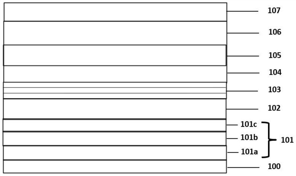
[0021] Please refer to figure 1 , A semiconductor laser element according to an embodiment of the present invention includes, from bottom to top, a substrate 100, an n-type cladding layer 101, a lower waveguide layer 102, an active layer 103, an upper waveguide layer 104, an electron blocking layer 105, a p-type The cladding layer 106 and the p-type semiconductor 107 .

[0022] Among them, the substrate 100 is a substrate on which nitride semiconductor crystals can be epitaxially grown, used to support each layer of epitaxial materials of the semiconductor laser element, and can be selected and used to satisfy the wavelength range of the light emitted by the semiconductor light emitting elemen...


PUM

PropertyMeasurementUnit
thicknessaaaaaaaaaa
temperatureaaaaaaaaaa
pressureaaaaaaaaaa

Abstract

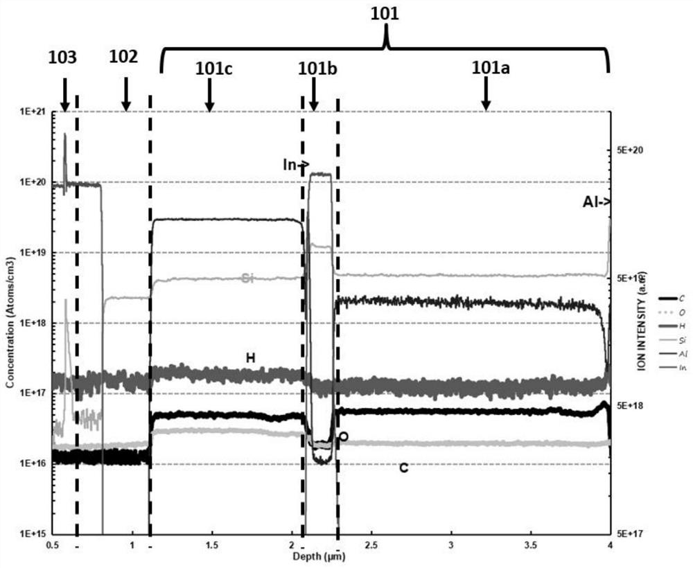
The invention relates to the technical field of semiconductor photoelectric devices, in particular to a semiconductor laser element which sequentially comprises a substrate, an n-layer coating layer, a lower waveguide layer, an active layer, an upper waveguide layer, an electron blocking layer, a p-type coating layer and a p-type semiconductor from bottom to top, the active layer is InbGa1-bN / IncAldGa1-c-dN, the n-type coating layer is at least provided with three Al gradient layers AleGa1-eN / AlfIngGa1-f-gN / AlhGa1-hN, al component e > h > f > = d, the In component gradient is formed by AlfIngGa1-f-gN and the In component gradient formed by the active layer, the upper waveguide layer and the lower waveguide layer, the polarization effect is regulated and controlled through double gradient combination, fluctuation and strain of the In component of the active layer are reduced, the gain spectrum width of the laser element is reduced, and the laser element is improved in performance. According to the present invention, the excitation intensity and the peak gain are improved, the thermal stability of the active layer is improved, the strong coupling effect of the exciton-photon at the room temperature is achieved, and the stable exciton polariton lasing is finally formed.

Description

technical field [0001] The present invention relates to the technical field of semiconductor optoelectronic devices, in particular to a semiconductor laser element with an n-type cladding layer for improving exciton polariton lasing. Background technique [0002] Lasers are widely used in display, communication, medical, weapons, guidance, ranging, cutting, welding and other fields. There are many types of lasers and various classification methods, mainly including solid, gas, liquid, semiconductor and dye lasers. Compared with other types of lasers, semiconductor lasers have the advantages of small size, light weight, long life and simple structure. There is a big difference between lasers and nitride semiconductor light-emitting diodes. 1) Lasers are generated by stimulated radiation of carriers, with a small spectral half-height width and high brightness. The output power of a single laser can be in the W level, while nitrogen The compound semiconductor light-emitting di...

Claims


Application Information

Patent Timeline
Patent Type & Authority Applications(China)
IPC IPC(8): H01S5/343H01S5/20
CPCH01S5/34333H01S5/2031
Inventor 阚钦
Owner 安徽格恩半导体有限公司
Learn More