Process for preparing carbon electrode array with high surface area and high gap filling capacity

A high-surface-area, carbon-electrode technology, applied in electrode manufacturing, chemical instruments and methods, photoplate-making process on patterned surfaces, etc., to achieve the effects of simple production, enhanced energy storage capacity, and low cost

Inactive Publication Date: 2005-11-30
TSINGHUA UNIV
View PDF0 Cites 15 Cited by
  • Summary
  • Abstract
  • Description
  • Claims
  • Application Information

AI Technical Summary

Problems solved by technology

At present, the laboratory led by Professor Madou has been able to manufacture a carbon electrode array with a thickness of 275 microns and an aspect ratio of 10:1 by using the SU-8 thick resist photolithography technology. However, using this technology will further increase the thickness of the photoresist. And to achieve an ideal aspect ratio will undoubtedly face severe challenges

Method used


Image

  • Process for preparing carbon electrode array with high surface area and high gap filling capacity

Examples


preparation example Construction

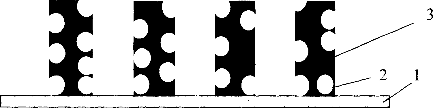
[0016] The present invention proposes a method for preparing a carbon electrode array with high surface area and high interstitial capacity. Its implementation consists of three steps:

[0017] 1) A high polymer expandable microsphere composed of a thermoplastic shell and a thermal expansion agent inside. The shell is a copolymer of monomers such as acrylonitrile and vinylidene chloride, and the thermal expansion agent is usually isobutane or isopentane. Add to photoresist for thick resist photolithography:

[0018] First add 0.1-30% volume percentage of polymer expandable microspheres into the photoresist and mix them uniformly, and then evenly coat them on silicon wafers, silicon nitride, silicon dioxide, quartz glass or metal linings, etc. On the bottom surface, the film thickness is about tens to hundreds of microns. After pre-baking, exposure, development and other photolithography processes, a patterned photoresist structure with a certain aspect ratio is formed;

[0...

Embodiment

[0025] Add high polymer expandable microspheres with a diameter of 6 microns to the SU-8 light by volume ratio of 5% by the thermoplastic shell of the copolymer of monomers such as acrylonitrile and vinylidene chloride and isobutane heat expansion agent. In the resist, mix evenly, and then evenly coat it on the surface of the silicon wafer substrate, the film thickness is about tens to hundreds of microns, after pre-baking, exposure, development and other photolithography processes, place it at a temperature of 80-300 ° Lower the pre-bake, control the upper limit of the temperature to 300°C, remove the organic solvent in the photoresist, place it in an open quartz tube heating furnace, feed 2000sccm of nitrogen gas and raise the temperature to 900°C at a heating rate of 10°C / min, Then modified 5% H 2 and N 2 The mixed gas is kept at 2000sccm for 1 hour, and finally 2000sccm of nitrogen gas is used to cool to room temperature, and the photoresist is subjected to pyrolytic carb...


PUM

PropertyMeasurementUnit
thicknessaaaaaaaaaa

Abstract

This invention relates to carbon electrode array process method with large surface area and filling capacity in the field of micro machine system and micro battery, which comprises the following steps: adding some percentage of highly polymers expansion balls into the light etching glue and mixing them evenly; then coating it evenly on silicon slice, silicon nitride, earth silicon, quartz glass or metal underlay bottom surfaces; through drying, exploring, developing procedures; forming one graph thick film etching glue layer with certain deepness to width proportion; then processing light etching glue thermal carbon and forming hollow hole on the carbon electrode array; finally forming carbon electrode array structure with large surface area and filling capacitor.

Description

technical field [0001] The invention belongs to the field of micro-electromechanical systems (MEMS) and micro-batteries, and particularly relates to a carbon electrode array with high surface area and high interstitial capacity, which has simple process and low cost, and can significantly improve the surface area and interstitial capacity at the same time Preparation. Background technique [0002] Lithium-ion battery is a kind of green and environment-friendly rechargeable battery with high energy density. At present, the positive electrode material of industrialized large-scale production of lithium-ion batteries is mainly lithium-intercalated transition metal oxides, and the negative electrode materials are basically carbon materials. The amount of current generated depends on the extent of the chemical reaction that takes place, which is closely related to the surface area of ​​the electrodes and the capacity of the electrolyte in the battery. Current reports of very hi...

Claims


Application Information

Patent Timeline
Patent Type & Authority Applications(China)
IPC IPC(8): B81C99/00H01M4/04
CPCY02E60/10
Inventor 岳瑞峰刘理天
Owner TSINGHUA UNIV
Why Eureka
Try Eureka