

Precious metal switch contact component and its preparation method
a technology of switch contact and component, which is applied in the field of switch contact components, can solve the problems of poor chemical stability, less ideal electrical conductivity of contact materials, and high price, and achieve the effects of better dust resistance, oil stain resistance, and reduced thickness or the height of protruding protruding parts
- Summary
- Abstract
- Description
- Claims
- Application Information
AI Technical Summary
Benefits of technology
Problems solved by technology
Method used
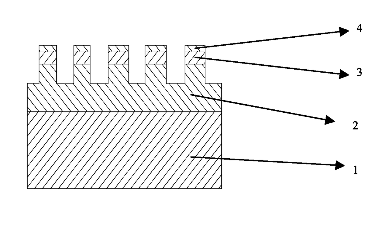
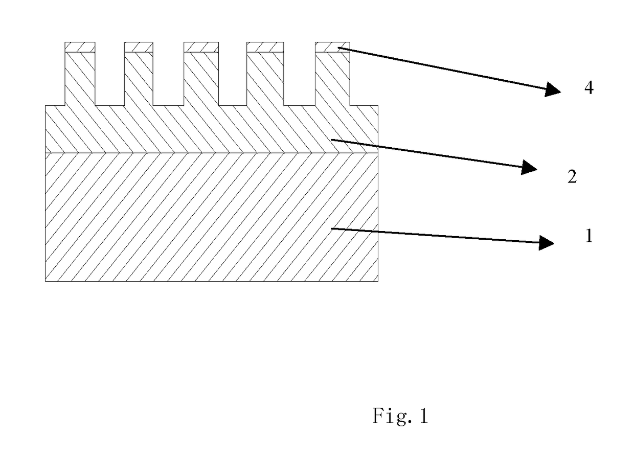
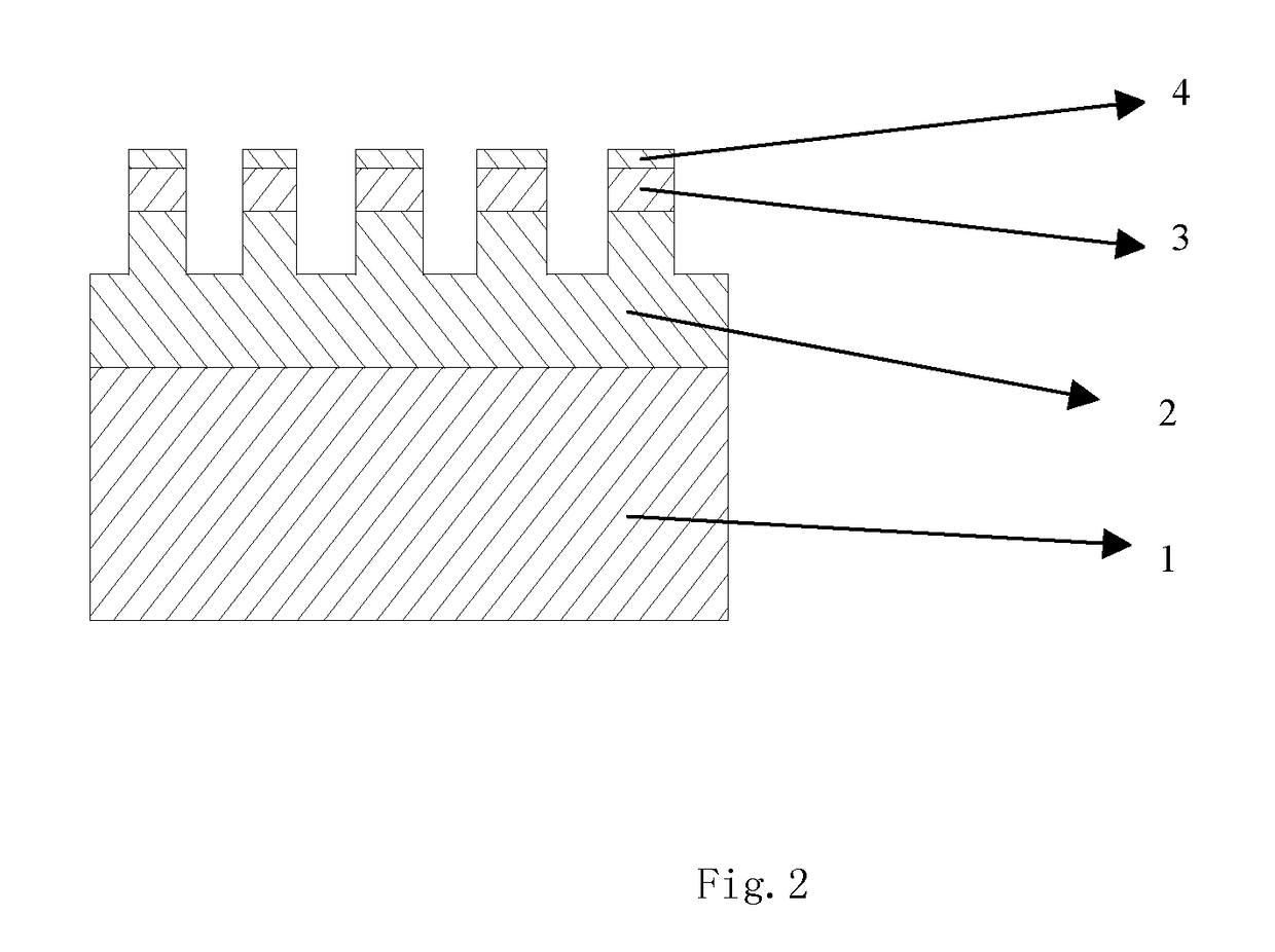
Image

Examples
example 1
[0060]Bonding of stainless steel and silicone rubber: a 0.10 mm thick SUS304 stainless steel sheet is cleaned by alkaline detergent to remove oil stain, then flushed with water, and then soaked in 5% dilute hydrochloric acid for 30 seconds, then washed out with deionized water. After drying by cold air, a methyl vinyl silicone rubber containing 1% vinyl tris(tert-butylperoxy) silane (VTPS) and 0.5% dicumyl peroxide (DCP) and the stainless steel sheet are placed in a mold cavity, whose surface had been coated with Teflon. and then one side of the stainless steel sheet is bonded with silicone rubber by thermal vulcanization at 175° C. for 8 minutes to form a 1.0 mm thick laminated composite of stainless steel and silicone rubber. Methyl vinyl silicone rubber such as SE 4706U produced by Dow Corning Toray, KE 961U produced by Shin Etsu or other brands available commercially are all usable. VTPS is a coupling agent containing peroxide, which can make the vinyl-containing silicone rubber...
example 2
[0066]On one side of the stainless steel sheet mentioned in Practical Example 1, the plating mask is applied, and the other side is fully covered with a plating mask of the same composition in the same thickness. And then gold plating is applied as specified in Practical Example 1. The plating mask on the gold plated side of the stainless steel sheet is cleaned off by 5% sodium hydroxide solution and then the etching process is carried out in a way as mentioned in Example 1. After that, the plating mask on another side of the stainless steel substrate is washed off by using 5% sodium hydroxide solution. The non-gold plated side of the stainless steel sheet and the silicone rubber are bonded by thermal vulcanization to form a 1 mm thick laminated composite sheet of stainless steel and silicone rubber with gold plated on the stainless steel surface. After punching of this laminated composite sheet, small pills in diameters of 2-10 mm are obtained. These small pills are to be used as t...
example 3
[0067]All the procedural steps are the same as in Example 1, except for the gold plating, which shall be changed to silver plating. The silver plating is prepared by either electroplating or electroless plating. The thickness of the silver plating is 2.5 μm. In order to prevent the discoloration of the silver plating, the silver plating layer can be subjected to post-treatments, such as bright-dipping, chemical and electrochemical passivation, coating with silver plating antioxidant or protective agent, etc.
PUM
| Property | Measurement | Unit |
|---|---|---|
| thickness | aaaaa | aaaaa |
| thickness | aaaaa | aaaaa |
| thickness | aaaaa | aaaaa |
Abstract
Description
Claims
Application Information