
Low thermal budget fabrication of ferroelectric memory using RTP

a ferroelectric memory and low thermal budget technology, applied in the direction of polycrystalline material growth, crystal growth process, chemistry apparatus and processes, etc., can solve the problems of deterioration of the electronic characteristics of the mosfet, economic unfeasibility, oxygen damage to the semiconductor substrate and other elements of the cmos circuit,

Inactive Publication Date: 2004-05-27
SYMETRIX
View PDF8 Cites 22 Cited by
  • Summary
  • Abstract
  • Description
  • Claims
  • Application Information

AI Technical Summary

Benefits of technology

[0012] Efforts in the prior art to reduce heating temperature or heating times commonly did not change the thickness of the ferroelectric thin film in a memory capacitor. Decreasing the thickness of the ferroelectric thin film, in accordance with the invention, contributes to reducing the minimal thermal budget of a process, that is, the minimal thermal budget value for achieving good electronic and circuit properties.
[0014] In accordance with the invention, the oxidation and crystallization of precursor compounds to form layered superlattice material, or other ferroelectric or dielectric metal oxide material, depends on numerous factors. These factors include: ramping rate, holding time, hold temperature, oxygen-content of the RTP atmosphere, composition of the liquid precursor and the desired metal oxide material, and thickness of a precursor coating and resulting thin film of layered superlattice material. Ferroelectric layered superlattice materials, like the metal oxides SrBi.sub.2Ta.sub.2O.sub.9 (SBT) and SrBi.sub.2(Ta.sub.1-xNb.sub.x)-.sub.2O.sub.9 (SBTN), where 0.ltoreq.x.ltoreq.1, are particularly useful in nonvolatile memory applications, such as in FeRAMs and nondestructible read-out ferroelectric FETs. Polycrystalline thin films of these layered superlattice materials, as well as other layered superlattice materials, may be fabricated in accordance with the invention. In accordance with the invention, RTP hold temperatures suitable for forming a layered superlattice material are in the range of about from 500.degree. C. to 900.degree. C., preferably from 550.degree. C. to 800.degree. C. For ferroelectric layered superlattice materials such as strontium bismuth tantalate, SrBi.sub.2Ta.sub.2O.sub.9, and strontium bismuth tantalate, SrBi.sub.2(Ta.sub.1-xNb.sub.x).sub.2O.sub.9, 0.ltoreq.x.ltoreq.1, conducting RTP treatments with a nominal ramping rate of 100.degree. C. / second and a cumulative holding time in a range of about 21 / 2 minutes (150 seconds) or less at hold temperatures in a range of about from 550.degree. C. to 750.degree. C. results in high remanent polarization, high breakdown voltage, low leakage current and low fatigue. Embodiments in accordance with the invention having a low thermal budget are also useful for providing a thin film of a metal oxide that is not a layered superlattice material, for example, an ABO.sub.3-type perovskite, such as barium strontium titanate.
[0015] In one aspect of the invention, it is not necessary to conduct any oxygen furnace anneals. Thus, in preferred embodiments in accordance with the invention, RTP treatment is the only heating technique performed at an elevated temperature above about 500.degree. C. to promote reaction and crystallization in the deposited thin film to form the desired polycrystalline layered superlattice material or other metal oxide. Because heating of a ferroelectric or a dielectric metal oxide thin film by RTP is very effective compared with other heating techniques, such as furnace annealing, the thermal budget of a method in accordance with the invention is minimized.
[0016] After the RTP has been conducted, the substrate containing the layered superlattice material thin film may optionally be given an oxygen furnace anneal. It is generally believed in the art that an oxygen furnace anneal conducted after an RTP tends to increase the remanent polarization of the layered superlattice material. Nevertheless, in one aspect of the invention, good electric properties and good physical properties of layered superlattice materials are achieved without a furnace anneal in either oxygen or in a nonreactive gas.

Problems solved by technology

As a result of the presence of reactive oxygen at elevated temperatures, numerous defects, such as dangling bonds, are generated in the crystal structure of the semiconductor silicon substrate, leading to deterioration in the electronic characteristics of the MOSFET.
Nevertheless, the total duration of annealing and other heating steps at 700.degree. C. to 900.degree. C. in methods disclosed in the prior art is typically in a range of about two to four hours or more, which may be economically unfeasible.
More importantly, long exposure times of 30 minutes or more in oxygen, even at the somewhat reduced temperature ranges, typically results in oxygen damage to the semiconductor substrate and other elements of the CMOS circuit.
After completion of the integrated circuit, the presence of oxides may still cause problems because oxygen atoms from a thin film of metal oxide layered superlattice material tend to diffuse through the various materials contained in the integrated circuit and combine with atoms in the substrate and in semiconductor layers, forming undesired oxides.
The resulting oxides interfere with the function of the integrated circuit; for example, they may act as dielectrics in the semiconducting regions, thereby forming virtual capacitors.
Diffusion of atoms from the underlying substrate and other circuit layers into the ferroelectric metal oxide is also a problem; for example, silicon from a silicon substrate and from polycrystalline silicon contact layers is known to diffuse into layered superlattice material and degrade its ferroelectric properties.
Nevertheless, as the market demand and the technological ability to manufacture high-density circuits increase, the distance between circuit elements decreases, and the problem of molecular and atomic diffusion between elements becomes more acute.
At temperatures in this range or higher for more than even a few minutes, the highesttemperature barrier materials quickly begin to degrade and to lose their diffusionbarrier properties.
Nevertheless, such prolonged heating at elevated temperature typically damages semiconductor substrate, conductive plugs, diffusion barriers and other elements of integrated circuits.
Fabrication of integrated circuits containing ABO.sub.3-type perovskites and other dielectric and ferroelectric metal oxides using processes at elevated temperatures as described above with reference to layered superlattice materials results in similar problems of undesired diffusion and structural damage, resulting in degradation of electronic properties.
It has been observed that damage to an integrated circuit resulting from heating at a given temperature decreases by reducing the duration of heating at that temperature.
Further, it has been observed that damage to the integrated circuit further decreases by utilizing RTP heating.
Damage from heating an integrated circuit also decreases by heating at an increased temperature for a shorter amount of time.
Nevertheless, the proportional relationship of reaction rate to temperature is usually not linear.
The reduced heating time at elevated temperature of a low-thermal-budget technique reduces the formation of hillocks and other non-uniformities at the surfaces of deposited layers.

Method used


Image

  • Low thermal budget fabrication of ferroelectric memory using RTP
  • Low thermal budget fabrication of ferroelectric memory using RTP
  • Low thermal budget fabrication of ferroelectric memory using RTP

Examples


example 2

[0093] A substrate wafer was prepared and ferroelectric capacitors were fabricated using a low thermal budget in accordance with the invention, as in Example 1, except that the liquid spin-on layer was spun at 2000 rpm instead of 2500 rpm. As a result, the ultra-thin film of SBT layered superlattice material had a thickness of about 35 nm, instead of 25 nm. The polarizability, expressed as the 2Pr-value, of the 35-nm capacitors was about 11.5 .mu.C / cm.sup.2 measured at 3 volts. The 2Pr-value measured at 1 volt was about 10.4 .mu.C / cm.sup.2 . The coercive voltage measured was about 0.3 volts, which corresponds to a coercive field, Ec, of about 170 kV / cm.

example 3

[0094] Ferroelectric capacitors containing an ultra-thin film of SBT layered superlattice material were fabricated using a low thermal budget in accordance with the invention by applying a single spin-on layer of liquid precursor on a substrate prepared as in Example 1. Thus, the cumulative heating time was about 2.5 minutes. The ultra-thin films of SBT had a thickness of about 48 nm. The fabrication conditions are summarized here:

2 Substrate: Si / SiO.sub.2 / Pt Solution: MOD Sr.sub.0.9Bi.sub.2.2Ta.sub.2O.sub.9, 0.08 molar Deposition: Spin-on, 1 layer @ 1500 rpm Baking: 1.sup.st plate @ 160.degree. C. / 1 min. 2.sup.nd plate @ 260.degree. C. / 4 min. Pre-TE RTP: 625.degree. C. / 30 sec. in O.sub.2 TE: 2000A Pt TE / FE etch: Dry etch Post-TE RTP: 750.degree. C. / 120 sec. in O.sub.2 Thermal budget: 118,750.degree. C.-sec

[0095] Another set of ferroelectric capacitors were fabricated in accordance with the invention on another substrate wafer by applying two spin-on layers of liquid precursor solut...

example 4

[0098] Ferroelectric capacitors containing a thin film of SBT layered superlattice material were fabricated using a low thermal budget in accordance with the invention by applying a single spin-on layer of liquid precursor on a substrate prepared as in Example 1. The thin films of SBT had a thickness of about 60 nm. The fabrication conditions are summarized here:

5 Substrate: Si / SiO.sub.2 / Pt Solution: MOD Sr.sub.0.9Bi.sub.2.2Ta.sub.2O.sub.9, 0.1 molar Deposition: Spin-on, 1 layer @ 2000 rpm Baking: 1.sup.st plate @ 160.degree. C. / 1 min. 2.sup.nd plate @ 260.degree. C. / 4 min. Pre-TE RTP: 625.degree. C. / 30 sec. in O.sub.2 TE: 200 nm Pt TE / FE etch: Dry etch Post-TE RTP: 700.degree. C. / 60 sec or 750.degree. C. / 120 sec. in O.sub.2 Thermal budget: 60,750.degree. C.-sec or 108,750.degree. C.-sec

[0099] Thus, the cumulative heating time at elevated temperature was about 1.5 min., or alternatively about 2.5 minutes. Additionally, a set of ferroelectric capacitors was fabricated using a "high t...


PUM


Abstract

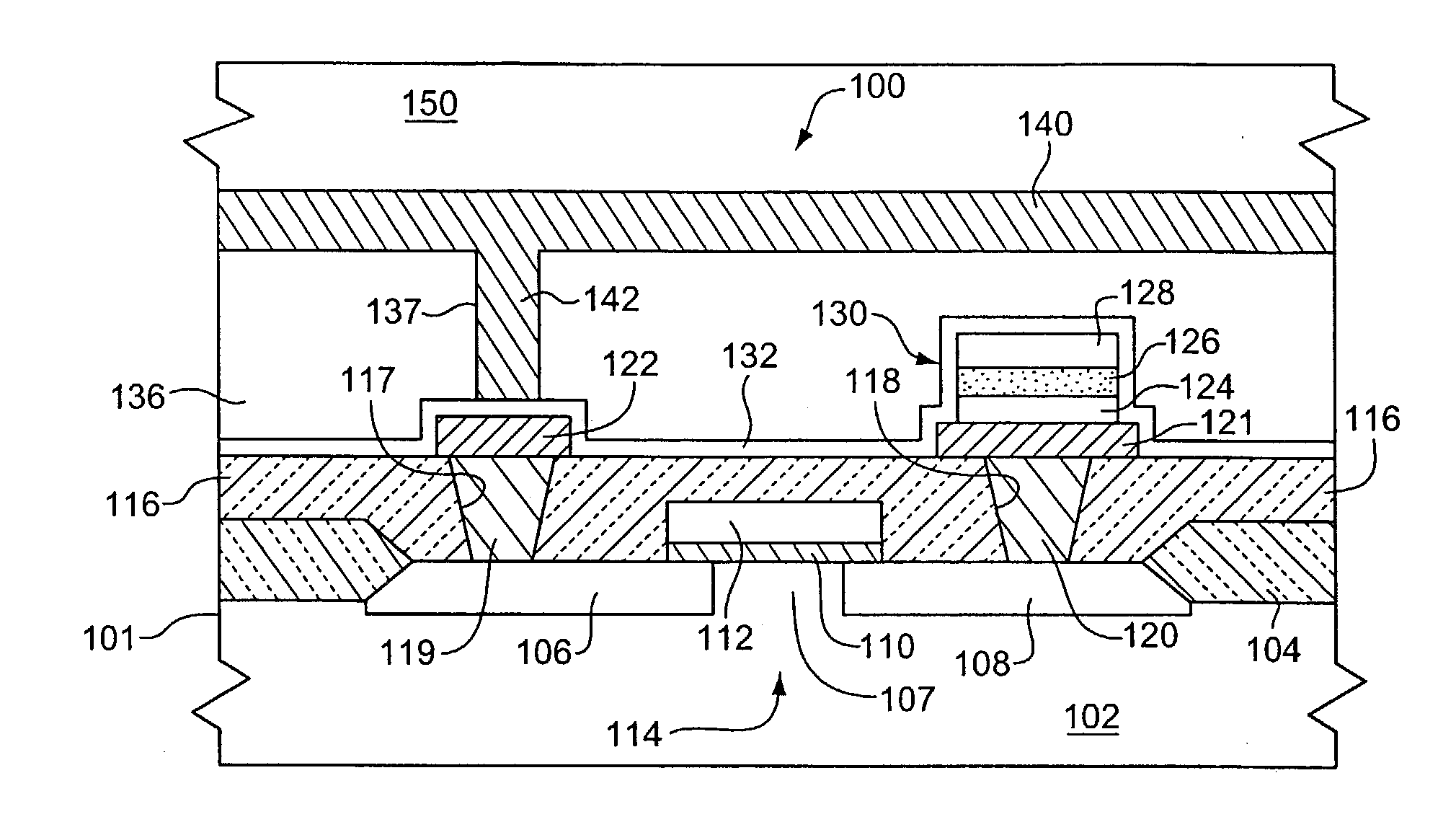
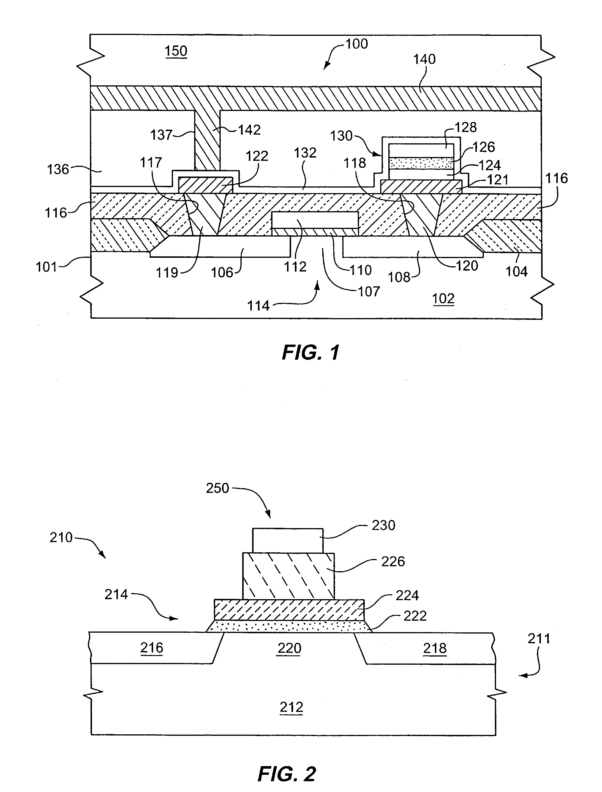
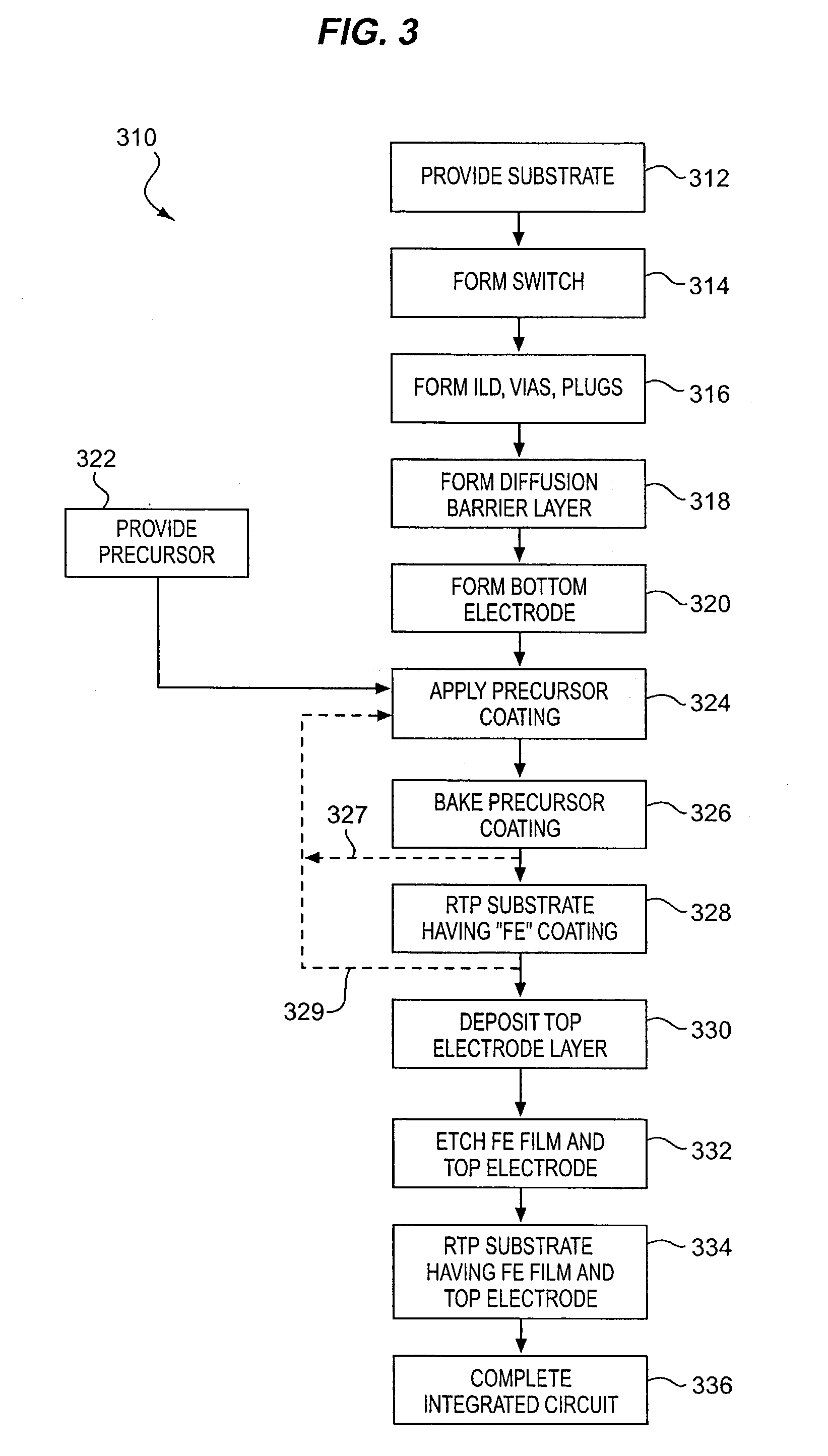
A precursor for forming a thin film of layered superlattice material is applied to an integrated circuit substrate. The precursor coating is heated using rapid thermal processing (RTP) with a ramping rate of 100° C. / second at a hold temperature in a range of from 500° C. to 900° C. for a cumulative heating time not exceeding 30 minutes, and preferably less than 5 minutes. In fabricating a ferroelectric memory cell, the coating is heated in oxygen using RTP, then a top electrode layer is formed, and then the substrate including the coating is heated using RTP in oxygen or in nonreactive gas after forming the top electrode layer. The thin film of layered superlattice material preferably comprises strontium bismuth tantalate or strontium bismuth tantalum niobate, and preferably has a thickness in a range of from 25 nm to 120 nm. The process of fabricating a thin film of layered superlattice material typically has a thermal budget value not exceeding 960,000° C.-sec, preferably less than 50,000° C.-sec.

Description

1. FIELD OF THE INVENTION[0001] The invention in general relates to the fabrication of dielectric and ferroelectric metal oxides in integrated circuits, and in particular, to the formation of nonvolatile integrated circuit memories containing ferroelectric layered superlattice materials.2. BACKGROUND OF THE INVENTION[0002] Ferroelectric compounds possess favorable characteristics for use in nonvolatile integrated circuit memories. See U.S. Pat. No. 5,046,043 issued Sep. 3, 1991 to Miller et al. A ferroelectric device, such as a capacitor, is useful as a nonvolatile memory when it possesses desired electronic characteristics, such as high residual polarization, good coercive field, high fatigue resistance, and low leakage current. Layered superlattice material oxides have been studied for use in integrated circuits. U.S. Pat. No. 5,434,102 issued Jul. 18, 1995 to Watanabe et al., and U.S. Pat. No. 5,468,684 issued Nov. 21, 1995, to Yoshimori et al., describe processes for integrating...

Claims


Application Information

Patent Timeline
IPC IPC(8): C30B29/32C30B29/68H01L21/02H01L21/314
CPCC30B29/32H01L28/55C30B29/68
Inventor CELINSKA, JOLANTAJOSHI, VIKRAMSOLAYAPPAN, NARAYANLIM, MYOUNGHOMCMILLAN, LARRY D.PAZ DE ARAUJO, CARLOS A.
Owner SYMETRIX
Learn More