Metal Pattern Forming Methd, Metal Pattern Obtained by the Same, Printed Wiring Board, Conductive Film Forming Method, and Conductive Film Obtained by the Same

a technology of metal pattern and conductive film, which is applied in the direction of metallic pattern materials, resistive material coatings, metallic material coating processes, etc., can solve the problems of high frequency characteristics deterioration, expensive apparatus such as a -ray generating apparatus and an electron beam generating apparatus, and achieve the effect of increasing the adhesion of metal layers according to the invention, eliminating incidences of exfoliation, and easy generation

Inactive Publication Date: 2007-10-25
FUJIFILM CORP +1
View PDF21 Cites 37 Cited by
  • Summary
  • Abstract
  • Description
  • Claims
  • Application Information

AI Technical Summary

Benefits of technology

[0041] As described above, the adhesiveness of metal layer according to the invention is increased, probably because radicals are generated and polymerization occurs only on the substrate surface, as a result of extremely smaller solubilization of the initiator component when a particular polymerization initiating layer is formed, suppressing the generation of the homopolymer not directly bonded to the substrate surface, eliminating incidences of exfoliation due to ablation or the like of the metal layer formed by plating.
[0042] In addition, the particular polymerization initiating layer has an advantage that there is no need for a large-scale facility, as the photopolymerization initiating group is connected to the polymer as a pendant and thus active species can be generate easily by an activated light such as UV or the like without use of an ultra-activated light such as plasma or γ ray.
[0043] In the invention, a metal pattern higher in resolution than those obtained by conventional pattern-forming methods of etching by using a resist pattern can be easily obtained because the region interactive with the electroless plating or the precursor thereof formed by the methods of embodiments (1) to (3) is provided selectively with an electroless plating catalyst or a precursor thereof and subsequently is subjected to electroless plating. The method is also advantageous in that there is no etching wastewater discharged.
[0044] In the invention, a surface graft layer (graft polymer layer) is formed by subjecting the substrate to a surface-grafting treatment (described below in detail). When the surface graft layer is added with an electroless plating catalyst or a precursor thereof and subjected to electroless plating, surface graft polymer chain contained in the surface graft layer, which is formed by polymerization from the substrate interface, has a larger motility and thus is more reactive with the electroless plating catalyst or precursor thereof. In addition, as the surface graft polymer chain has a higher motility, the electroless plating bath penetrates more easily into the layer, allowing the electroless plating to proceed on and inside the surface graft layer. As a result, the metal pattern or metal layer (conductive film) on the surface become in the hybrid state with the surface graft polymer chain directly bonded to the substrate. In the invention, modification of the substrate surface by the surface-grafting treatment in this manner seems to minimize the surface roughness of the substrate surface where the metal patterned area or the metal layer (conductive film) is formed, and a metal layer superior in adhesiveness is formed on such a smooth substrate surface probably due to the hybrid state described above.
[0045] In addition, when surface graft polymerization is carried out on the particular polymerization initiating layer, generation of homopolymer not bonded to the substrate is seemingly suppressed and the adhesiveness between the metal pattern or metal layer (conductive film) formed and the substrate is increased drastically.
[0046] When the metal pattern or the conductive film obtained by the method according to the invention is used for electric wiring, smaller interface roughness of the interface between the formed conductive area (plating catalyst, plating metal layer) and the organic material (graft polymer chain) leads to smaller electric loss during high-frequency electric transmission (transmission loss).

Problems solved by technology

As a result, the substrate interface of the metal pattern formed became rough, often causing a problem of deterioration in high frequency characteristics when the product is used for electric wiring.
In addition, it also carried the problem of requiring a complicated step of treating the substrate with a strong acid such as chromic acid or the like, as surface roughening of the substrate is required before forming the metal substrate.
However, an expensive apparatus such as a γ-ray generating apparatus and an electron beam generating apparatus is necessary.
Accordingly, even if a metal substrate prepared by this method is patterned by the subtractive method, the product still contained a problem inherent to the subtractive method as follows.
However, when a fine metal pattern is directly formed by the over-etching method, it was difficult to form a metal pattern having a line width of 30 μm or less from the practical viewpoint of forming a favorable fine metal pattern, due to the defects of the wire formed such as bleeding, thinning, disconnection, and the like.
In addition, it also carried the problems in cost and environmental friendliness, as it demanded removal of the metal film present in the area other than the patterned area, and it also required a significant cost for processing the metal wastewater from the etching treatment.
However, the method demands roughening of substrate surface for improvement in the adhesiveness between the substrate and the metal pattern, and as a result, the substrate interface of the metal pattern formed became rough, causing a problem of deterioration in the high frequency characteristics of product when it is used for electric wiring.
The fully-additive method allows easier formation of a thin line pattern having a line width of 30 μm or less as it is an etching-less process; and it also made the substrate interface rough in a similar manner to the semi-additive method, causing a problem of deterioration in the high frequency characteristics of product when it is used for electric wiring.
However, status quo, roughness of several microns interferes finer wiring.

Method used


Image

  • Metal Pattern Forming Methd, Metal Pattern Obtained by the Same, Printed Wiring Board, Conductive Film Forming Method, and Conductive Film Obtained by the Same
  • Metal Pattern Forming Methd, Metal Pattern Obtained by the Same, Printed Wiring Board, Conductive Film Forming Method, and Conductive Film Obtained by the Same
  • Metal Pattern Forming Methd, Metal Pattern Obtained by the Same, Printed Wiring Board, Conductive Film Forming Method, and Conductive Film Obtained by the Same

Examples


embodiment (

3)

[0254] Embodiment (3) include a step (I-3-1) of forming on a base material a photosensitive layer containing a light to heat conversion substance and a binder, and forming a polymer layer by chemically bonding a polymer having a functional group that interacts with an electroless plating catalyst or a precursor thereof directly onto the entire surface of the photosensitive layer, and a step (I-3-2) of forming, in the pattern form, a polymer layer that interacts with the electroless plating catalyst or precursor thereof by irradiating the polymer layer with radiation in the pattern form and ablating the photosensitive layer.

[0255] Hereinafter, the steps in embodiment (3), (I-3-1) and (I-3-2), are described respectively.

[0256] The step (I-3-1) in embodiment (3) step is first described.

[0257] Step (I-3-1) in embodiment (3) is a step of forming on a base material a photosensitive layer containing a light to heat conversion substance and a binder (hereinafter, the photosensitive lay...

example 1

(Preparation of Substrate)

[0369] The following composition was applied onto the surface of a base material, polyimide film (product name: Kapton, manufactured by Du Pont-Toray) by using a coating bar of rod No. 10 and dried at 100° C. for 1 minute, to give an intermediate layer having a thickness 1.6 μm and containing an infrared absorbent, which was used as substrate A in Example 1.

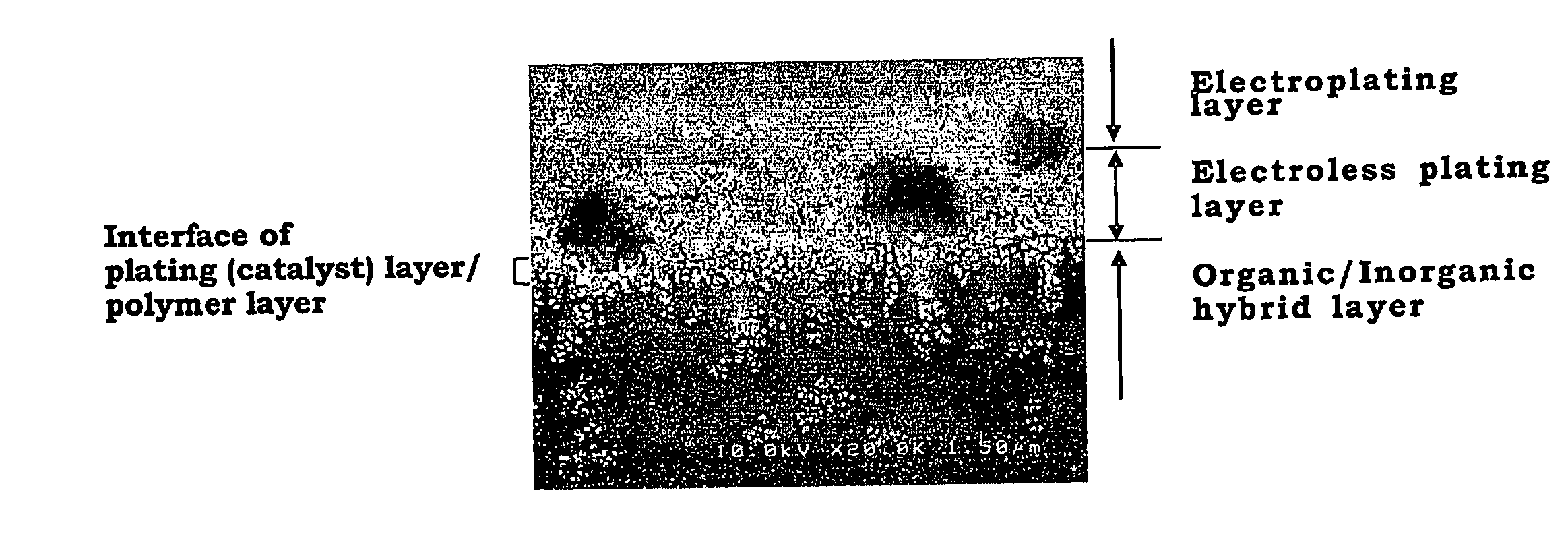
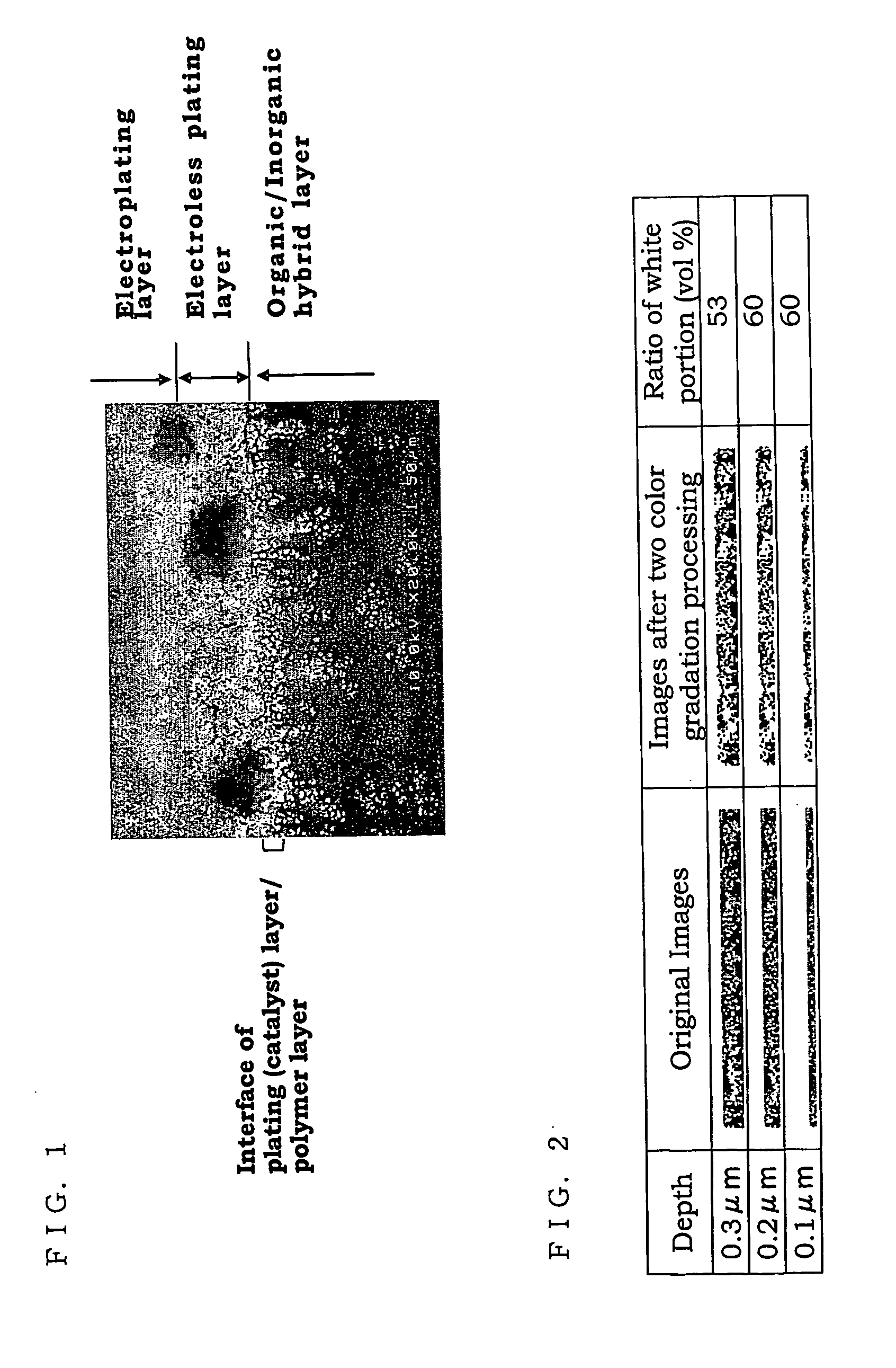
[0370] The Rz of the base material, polyimide film, as determined by measuring the surface in the range of 40 μm×40 μm according to the method specified in JIS B 0601 and by using Nanopics 1000 (manufactured by Seiko Instruments Inc.) was 15 nm. When the surface of substrate A having an intermediate layer formed on the polyimide film was also measured in a similar manner, the Rz was 10 nm, indicating that the surface roughness of substrate A used in Example was within the preferable range of the invention.

[0371]

Epoxy resin (Epikote, Yuka-shell Co, Ltd.)2 gInfrared absorbent (IR125, manufactured by0.2...

example 2

(Preparation of Substrate)

[0378] The following intermediate layer coating solution (photopolymerization composition) was applied onto the surface of a base material, the polyimide film used in Example 1, by using a rod bar of No. 18, dried at 80° C. for 2 minutes, to give an intermediate layer having a film thickness of 6 μm.

[0379] Then, the base material having the intermediate layer above was exposed to light by using a 400 W high-pressure mercury lamp (Type: UVL-400P, manufactured by Riko Kagaku Sangyo) for 10 minutes allowing partial hardening, to give substrate B used in Example 2.

[0380] The Rz of substrate B, as determined in a similar manner to the polyimide film base material, was 12 nm, indicating that the surface roughness of substrate B used in the Example was within the preferable range of the invention.

[0381]

Allyl methacrylate / methacrylic acid copolymer (copolymerization  2 gmolar ratio: 80 / 20, average molecular weight: 100,000)Ethylene oxide-modified bisphenol A d...


PUM

PropertyMeasurementUnit
surface roughnessaaaaaaaaaa
dielectric constantaaaaaaaaaa

Abstract

The present invention provides a method of forming a metal pattern and a metal pattern obtained by the method. The method includes the steps of (I) forming on a substrate a polymer layer in which a polymer having a functional group that interacts with an electroless plating catalyst or a precursor thereof is chemically bonded directly to the substrate in a pattern form, (II) adding the electroless plating catalyst or precursor thereof to the polymer layer, and (III) forming a metal layer in the pattern form by electroless plating. The present invention also provides a method of forming a conductive film, including the steps of (A) forming on a substrate a polymerization initiating layer in which a polymer having, on a side chain thereof, a crosslinking group and a functional group having polymerization initiating capability is immobilized by a crosslinking reaction on the surface of the base material, (B) generating a graft polymer by chemically bonding a polymer having a functional group that interacts with an electroless plating catalyst or a precursor thereof directly onto the entire surface of the polymerization initiating layer, (C) adding the electroless plating catalyst or precursor thereof to the graft polymer, and (D) forming a metal layer by electroless plating.

Description

FIELD OF THE INVENTION [0001] The present invention relates to a method of forming a metal pattern, a metal patter obtained thereby, a printed wiring board, a conductive film forming method, and conductive film obtained by the same. In particular, the present invention relates to a method of forming a metal pattern useful as a metal wiring board, a printed wiring board and the like, a metal pattern obtained by using the method, a printed wiring board, a method of forming a conductive film, and a conductive film obtained by using the method. BACKGROUND OF THE INVENTION [0002] Three major conventional metal pattern forming methods known in the art are “subtractive method”, “semi-additive method”, and “fully-additive method”. [0003] The subtractive method includes steps of forming a photosensitive layer sensitive to activated light irradiation over a metal layer formed on a substrate, exposing the photosensitive layer imagewisely, forming a resist image by developing, forming a metal p...

Claims


Application Information

Patent Timeline
Patent Type & Authority Applications(United States)
IPC IPC(8): H05K1/09B05D5/12C23C18/28G03F7/004G03F7/031G03F7/095G03F7/26G03F7/40H05K3/18
CPCG03F7/0045G03F7/031G03F7/095G03F7/0955G03F7/265C23C18/2086H05K3/185C23C18/1608C23C18/1612C23C18/1653C23C18/204G03F7/405
Inventor KANO, TAKEYOSHIKAWAMURA, KOICHI
Owner FUJIFILM CORP
Why Eureka
Try Eureka