Nanowires and nanoribbons as subwavelength optical waveguides and their use as components in photonic circuits and devices

a technology of nanowires and nanoribbons, applied in the field of optical waveguides, can solve the problems of unexplored optical integration, difficult and costly lithographic processes, and difficulty in assembly itsel

Inactive Publication Date: 2009-10-22
RGT UNIV OF CALIFORNIA
View PDF6 Cites 29 Cited by
  • Summary
  • Abstract
  • Description
  • Claims
  • Application Information

AI Technical Summary

Benefits of technology

[0015]The present invention is directed at assembling photonic circuits from a collection of nanoribbon / nanowire elements that assume different functions, such as light creation, routing and detection. The subwavelength optical waveguides of the invention are formed from a nanoribbon or nanowire having a diameter that is less than the wavelength of light to be guided and are potentially simpler while being versatile, such as serving as a fundamental element of photonic circuits of various types.

Problems solved by technology

Since nanowire synthesis and device assembly are typically separate processes, nanowires permit more flexibility in the heterogeneous integration of different materials than standard silicon technology allows, although the assembly itself remains a major challenge.
While the electrical integration of simple nanowire circuits using lithography has been demonstrated, optical integration, which promises higher speeds and greater device versatility, remains unexplored.
However, both of these approaches typically rely on difficult and costly lithographic processes for device fabrication and are in their early stages of development.
Optical spectroscopy is a powerful analytical tool for characterizing biological and chemical systems, but making a standard optical laboratory portable is a major challenge.
However, engineering versatile, reusable optical devices from materials such as photonic crystals and metallic nanostructures remains challenging due to the difficulty in performing spectroscopy with the guided optical energy.
In addition, the synthetic steps for producing these materials tend to be labor-intensive and involve costly lithographic techniques.
Though these various sensing configuration are promising for high sensitivity, fast cycling times and reversibility, they do not provide versatility in their spectroscopic detection or enable a chemical read-out of the analyte.

Method used


Image

  • Nanowires and nanoribbons as subwavelength optical waveguides and their use as components in photonic circuits and devices
  • Nanowires and nanoribbons as subwavelength optical waveguides and their use as components in photonic circuits and devices
  • Nanowires and nanoribbons as subwavelength optical waveguides and their use as components in photonic circuits and devices

Examples


example 3

8.1 Example 3

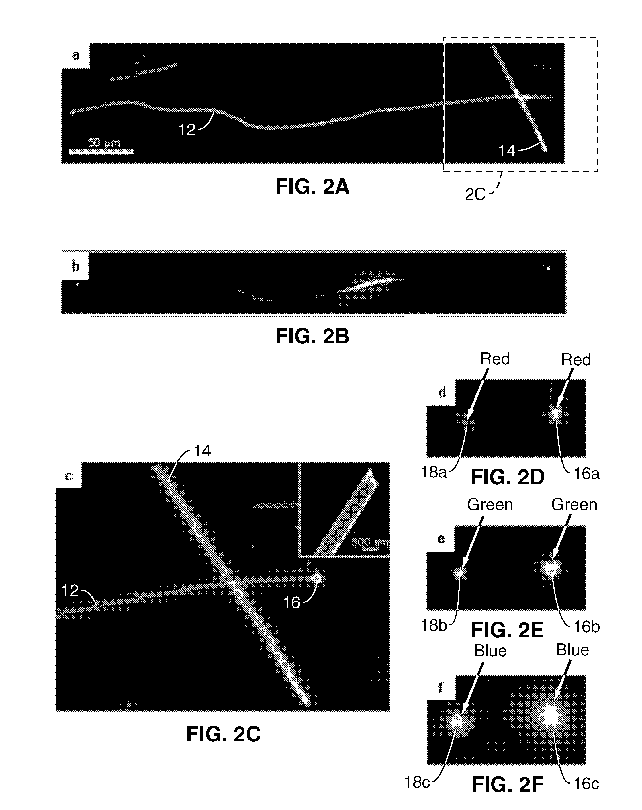
[0165]SnO2 nanoribbons were synthesized by the chemical vapor transport of SnO at 1100° C. in flowing argon. ZnO nanowires were grown as epitaxial arrays on sapphire substrates by the oxidation of metallic zinc at 800° C., using gold as a catalyst. GaN nanowires were made by the chemical vapor transport of gallium in a NH3 / H2 mixture at 900° C., with nickel as the catalyst. The SnO2 nanoribbons were dry transferred en masse to oxidized silicon substrates (600 nm SiO2, Silicon Sense Inc.). A triple-axis micromanipulator tipped with a tungsten probe (˜400 nm tip diameter) was used to remove individual ZnO and GaN nanowires (chosen by their PL spectra) from their growth substrates and then deposit them with the nanoribbons.

example 4

8.2 Example 4

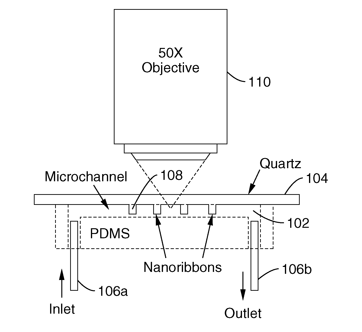
[0166]Nanoribbons and nanowires were manipulated with the probe under a dark-field microscope. A HeCd laser provided continuous wave (CW) resonant illumination (325 nm), while the fourth-harmonic of a Nd:YAG laser (266 nm, 8 nm, 10 Hz) was used for pulsed pumping. Laser diodes (652 nm and 532 nm) and the HeCd laser (442 nm) supplied visible light for the filtering and fluorescence demonstrations. The lasers were focused to a beam diameter of approximately 50 μm, giving a CW power density of approximately 175 W / cm2 and a pulsed energy density of approximately 10 μJ / cm2. Spectra were acquired with a fiber-coupled spectrometer (gratings at 150 and 1200 grooves / mm, SpectraPro 300i, Roper Scientific) and liquid N2-cooled CCD setup. Black-and-white and color images were recorded with two microscope-mounted CCD cameras (CoolSnap fx and CoolSnap cf, Photometrics).

[0167]Many of the nanoribbons / wires described herein operated as single-mode fibers for some of the experimental wav...

example 1

10.1 Example 1

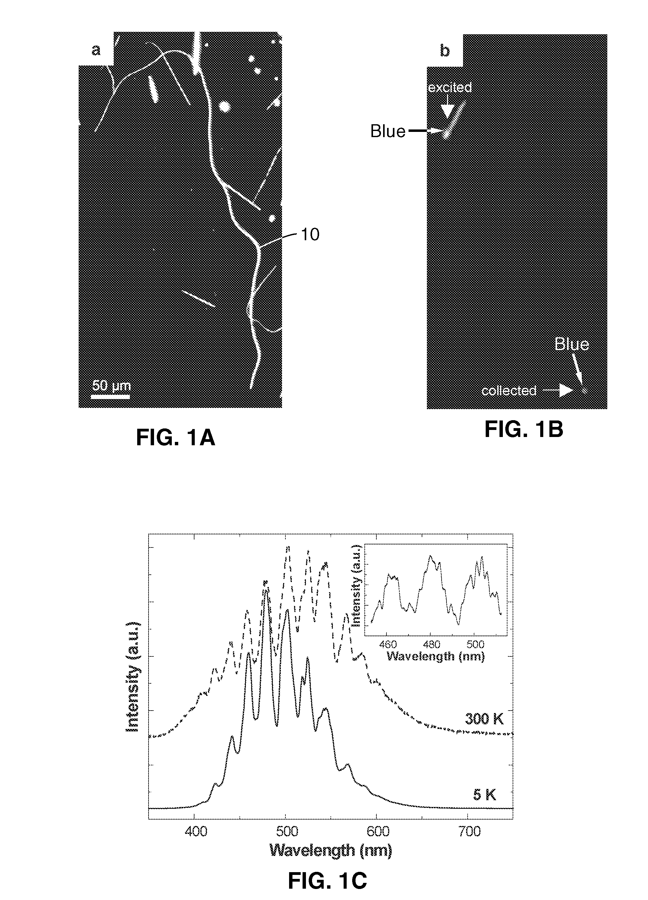
[0193]Tin dioxide (SnO2) nanoribbons were synthesized through a chemical vapor transport process. An alumina boat filled with tin monoxide powder was heated (1100° C.) in an alumina tube under a continuous flow of argon (300 torr) for approximately 2 hours. After removing the boat from the tube furnace, the nanoribbons were deposited on a clean glass substrate for optical characterization (see below). For surface enhanced Raman spectroscopy (SERS) detection, silver nanocrystals were prepared using a modified polyol process in which silver nitrate is reduced in a solution of 1,5-pentanediol (˜190° C.) in the presence of a capping polymer.

[0194]These tests were performed with an upright dark-field microscope operating in reflection mode. Monochromatic laser light was focused onto the sample at a 35° angle normal to the substrate. Broadband light (FWHM>200 nm) was generated in the waveguide by exciting the SnO2 nanoribbon with the 325 nm line of a continuous-wave HeCd las...


PUM

PropertyMeasurementUnit
aspect ratioaaaaaaaaaa
diameteraaaaaaaaaa
diameteraaaaaaaaaa

Abstract

A microfluidic optical sensor utilizes at least one subwavelength nanowire or nanoribbon waveguide coupled to a fluidic structure having at least one nanofluidic channel through which one or more molecular species are conveyed. In response to optical pumping (e.g., a laser source) the waveguide optically interrogates nearby molecular species retained within said fluidic structure to detect chemical species in response to optical characterization of small (on the order of sub-picoliter) volumes of solution. Characterization is performed in response to evanescent wave sensing. In one aspect, optical characterization is selected from the group of optical characterizations consisting of absorbance, fluorescence and surface enhanced Raman spectroscopy (SERS).

Description

CROSS-REFERENCE TO RELATED APPLICATIONS[0001]This application claims priority from, and is a 35 U.S.C. § 111(a) continuation of, co-pending PCT international application serial number PCT / US2007 / 078021, filed on Sep. 10, 2007, incorporated herein by reference in its entirety, which claims priority from U.S. provisional patent application Ser. No. 60 / 844,015 filed on Sep. 11, 2006, incorporated herein by reference in its entirety. This application is also a continuation-in-part of U.S. patent application Ser. No. 11 / 559,244 filed on Nov. 13, 2006, incorporated herein by reference in its entirety, which claims priority to U.S. provisional patent application Ser. No. 60 / 844,015 filed on Sep. 11, 2006. Priority is claimed to each of the foregoing applications.[0002]This application is related to PCT Publication No. WO 2008 / 033763, published on Mar. 20, 2008, incorporated herein by reference in its entirety.STATEMENT REGARDING FEDERALLY SPONSORED RESEARCH OR DEVELOPMENT[0003]This inventi...

Claims


Application Information

Patent Timeline
Patent Type & Authority Applications(United States)
IPC IPC(8): G01N21/00
CPCB01L3/5027B82Y15/00B82Y20/00G01N21/05G01N2021/0346G01N21/6489G01N21/658G01N21/7703G02B6/107G01N21/648
Inventor YANG, PEIDONGSIRBULY, DONALD J.FAN, RONGLAW, MATTHEWTAO, ANDREA
Owner RGT UNIV OF CALIFORNIA
Why Eureka
Try Eureka