Semiconductor device and method for fabricating the same

Inactive Publication Date: 2000-06-20
SEMICON ENERGY LAB CO LTD
View PDF57 Cites 256 Cited by
  • Summary
  • Abstract
  • Description
  • Claims
  • Application Information

AI Technical Summary

Problems solved by technology

However, it has been the fact that it is difficult to obtain a required crystallinity across the wide area through the heat treatment because it may cause nonuniformity in the crystallization.
Further, although it is possible to obtain the high crystallinity partly by irradiating laser light, it is difficult to obtain a good annealing effect across the wide area.
In this case, the irradiation of the laser light is apt to become unstable under the condition for obtaining specifically a good crystallinity.
However, because the metal element is contained within or on the surface of the crystal silicon film, the amount thereof to be introduced has to be controlled very carefully, thus posing a problem in its reproducibility and stability (electrical stability of a device obtained).
Specifically, there is a problem that an elapsed change of the characteristics of a semiconductor device to be obtained is large or an OFF value, in case of a thin film transistor, is large, due to the influence of the remaining metal element.
That is, although the metal element which promotes the crystallization of silicon plays the valuable and useful role in obtaining the crystal silicon film, its existence becomes a minus factor which causes various problems after obtaining the crystal silicon film once.
However, because it has a limit that a substrate composing the liquid crystal display needs to be translucent, its type is limited.
However, among them, the plastic substrate has a problem that it lacks in heat resistance and the quartz substrate has a problem that it is very expensive and its cost is more than 10 times of the glass substrate especially when it is widened, thus lacking in cost performance, though it can withstand a high temperature of about 1000.degree. C. or 1100.degree. C.
That is, because the heat resistant temperature of the glass substrate is normally about 600.degree. C., though it depends on a type thereof, a process which exceeds the heat resistant temperature of the glass substrate cannot be adopted in the step for forming the crystal silicon film.
However, the crystal silicon film crystallized from the amorphous silicon film by the above-mentioned technologies has had a large number of defects caused by dangling bond and the like.
The defects at the grain boundary in particular are the greatest factor of scattering charge, but it is very difficult to passivate the defects at the grain boundary.
In contrary to that, it is difficult to implement the heat treatment in high temperature

Method used


Image

  • Semiconductor device and method for fabricating the same
  • Semiconductor device and method for fabricating the same
  • Semiconductor device and method for fabricating the same

Examples


first embodiment

[First Embodiment]

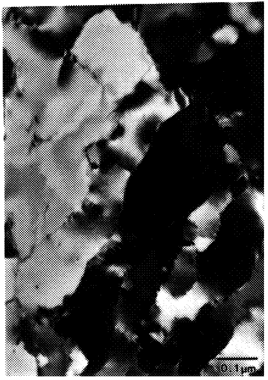
FIG. 14 shows a measured result of the distribution of concentration of nickel element in a direction of section of a crystal silicon film obtained by utilizing nickel as the metal element. This measurement was carried out by SIMS (secondary ion mass spectrometry). Steps for fabricating the sample from which these measured values have been obtained will be explained below briefly.

A silicon oxide film is formed as an underlying film in a thickness of 4000 angstrom on a quartz substrate and then an amorphous silicon film is formed in a thickness of 500 angstrom by low pressure thermal CVD. Next, nickel element is introduced to the amorphous silicon film by using nickel acetate aqueous solution. Further, the amorphous silicon film is crystallized by a heat treatment at 650.degree. C. for four hours to obtain a crystal silicon film. After that, another heat treatment is implemented within an oxidizing atmosphere at 950.degree. C. to form a thermal oxide film 500 angstr...

second embodiment

[Second Embodiment]

Next, as another method for forming the thermal oxide film, a heat treatment is implemented within an oxidizing (e.g. oxygen) atmosphere containing 3 volume % of HCl to form the thermal oxide film 500 angstrom thick. FIG. 15 shows measured data of this sample. As it is apparent from FIG. 15, the concentration of nickel within the crystal silicon film (poly-Si) is reduced further and instead of that, the concentration of nickel within the thermal oxide film is increased. This means that the nickel element has been sucked out (i.e. gettered) to the thermal oxide film.

The difference between FIG. 14 and FIG. 15 is only whether HCl has been contained within the atmosphere in forming the thermal oxide film. Accordingly, it can be concluded that HCl is related significantly with the above-mentioned effect of gettering, beside oxygen. Further, because no gettering effect is confirmed by H (hydrogen) which is a component of HCl, it can be seen that, more accurately, the ge...

third embodiment

[Third Embodiment]

A third embodiment relates to a case when an amorphous silicon film formed by plasma CVD is utilized instead of the amorphous silicon film which is the starting film of the crystal silicon film from which the data described in the first and second embodiments have been obtained. The other fabrication conditions are the same with those in the first embodiment. Because the quality of the amorphous silicon film formed by the plasma CVD is different from that of the amorphous silicon film formed by the low pressure thermal CVD, the action of gettering exerted after forming the crystal silicon film is also different.

FIG. 17 shows measured data of a sample in which the thermal oxide film has been formed in an oxygen atmosphere at 950.degree. C. As it is apparent from FIG. 17, although the nickel element has moved to the thermal oxide film, the nickel element exists relatively in high concentration within the crystal silicon film (poly-Si). It is noted that although the c...


PUM


Abstract

A novel and very useful method for forming a crystal silicon film by introducing a metal element which promotes crystallization of silicon to an amorphous silicon film and for eliminating or reducing the metal element existing within the crystal silicon film thus obtained is provided. The method for fabricating a semiconductor device comprises steps of intentionally introducing the metal element which promotes crystallization of silicon to the amorphous silicon film and crystallizing the amorphous silicon film by a first heat treatment to obtain the crystal silicon film; eliminating or reducing the metal element existing within the crystal silicon film by implementing a second heat treatment within an oxidizing atmosphere; eliminating a thermal oxide film formed in the previous step; and forming another thermal oxide film on the surface of the region from which the thermal oxide film has been eliminated by implementing another thermal oxidation.

Description

1. Field of the InventionThe present invention relates to a semiconductor device typified by a thin film transistor and to a fabrication method thereof. The present invention also relates to a semiconductor device using a crystal silicon thin film formed on a substrate such as a glass substrate and quartz substrate and to a fabrication method thereof. Further, the present invention relates to an insulated gate type semiconductor device such as a thin film transistor and to a fabrication method thereof.2. Description of Related ArtHitherto, there has been known a thin film transistor using a silicon film, i.e. a technology for forming the thin film transistor by using the silicon film formed on a glass substrate or quartz substrate. The glass substrate or quartz substrate is used as the substrate because the thin film transistor is used for an active matrix liquid crystal display. While a thin film transistor has been formed by using an amorphous silicon film (a-Si) in the past, it i...

Claims


Application Information

Patent Timeline
IPC IPC(8): H01L21/02H01L21/20H01L21/336H01L29/66H01L29/786H01L21/322H01L21/70H01L27/12H01L21/84H01L29/49H01L29/40H01L21/28H01L21/324H01L21/77
CPCH01L21/2022H01L21/28158H01L21/3221H01L21/3226H01L27/12H01L27/1277H01L29/66757H01L29/66765H01L29/78621H01L29/78675H01L27/1203H01L29/4908H01L21/02672H01L21/02686H01L21/02532H01L21/18
Inventor YAMAZAKI, SHUNPEITERAMOTO, SATOSHIKOYAMA, JUNOGATA, YASUSHIHAYAKAWA, MASAHIKOOSAME, MITSUAKIOHTANI, HISASHIHAMATANI, TOSHIJI
Owner SEMICON ENERGY LAB CO LTD
Why Eureka
Try Eureka