Method for processing surface of sample

a technology of surface treatment and sample, which is applied in the direction of electrical discharge tubes, decorative arts, electrical equipment, etc., can solve the problems of high production cost, uneven etching surface, and difficulty in etching films with gate electrodes having different conductivities

Inactive Publication Date: 2003-12-09
HITACHI LTD
View PDF27 Cites 27 Cited by
  • Summary
  • Abstract
  • Description
  • Claims
  • Application Information

AI Technical Summary

Problems solved by technology

Since the current technology is not sufficient to form metallic film directly on the oxide film, this method provides a way of forming polycrystalline silicon film on the oxide film, and forming and metal film thereon.
Etching of the film with multilayer architecture as discussed above raises new problems which are caused by etching reaction between the polycrystalline silicon and metal.
Then metal or barrier film remain unevenly on the polycrystalline silicon, causing irregularities on the etching surface.
Etching of the film with gate electrodes having different conductivities involves unprecedented issues.
For example, increase in the number of photolithographic processes to perform independent etching of p-type and n-type gates will result in higher production costs.
However, simultaneous etching of both p- and n-type gates will cause earlier exposure of the underlying gate oxide film on the n-type side since the etching rate of the n-type polycrystalline silicon is higher; this will result in a thinner oxide film on the n-type side or separation of oxide film on the n-type side.
One of the ensuing problems to be solved relates to the mask to form very small patterns.
So the resist itself provides a groove with a higher aspect ratio, resulting in more difficult processing of a narrow groove.
However, processing of a very thin hard mask involves a new problem of requesting further improvement of the selectivity between the underlying substance as an etched material and hard mask.
In the processing of such minute patterns, the line is gradually increased in thickness and the pattern cannot be designed to have the design dimensions.
This will create a serious issue.
Furthermore, in addition to the differences of etching rate inside the minute groove and on the wider portion, differences in shape, so-called microloading will present a serious issue, which will cause processing failure.
In such a device, a trade-off relationship is established in selectivity between anisotropy and underlying oxide film, and this makes processing more difficult.
These inventions are finding it difficult to cope with processing of more minute elements.
Processing of such minute elements requires assembling under compact process conditions based on analysis of the relationship between the physical volume of plasma and etching characteristics, and many manufacturers are currently spending a lot of time and labor in this direction.
However, setting of ion to a higher value will increases the etching rate of the oxide film, and this is unfit for processing of a gate electrode where underlying oxide film is thin.

Method used


Image

  • Method for processing surface of sample
  • Method for processing surface of sample
  • Method for processing surface of sample

Examples


first embodiment

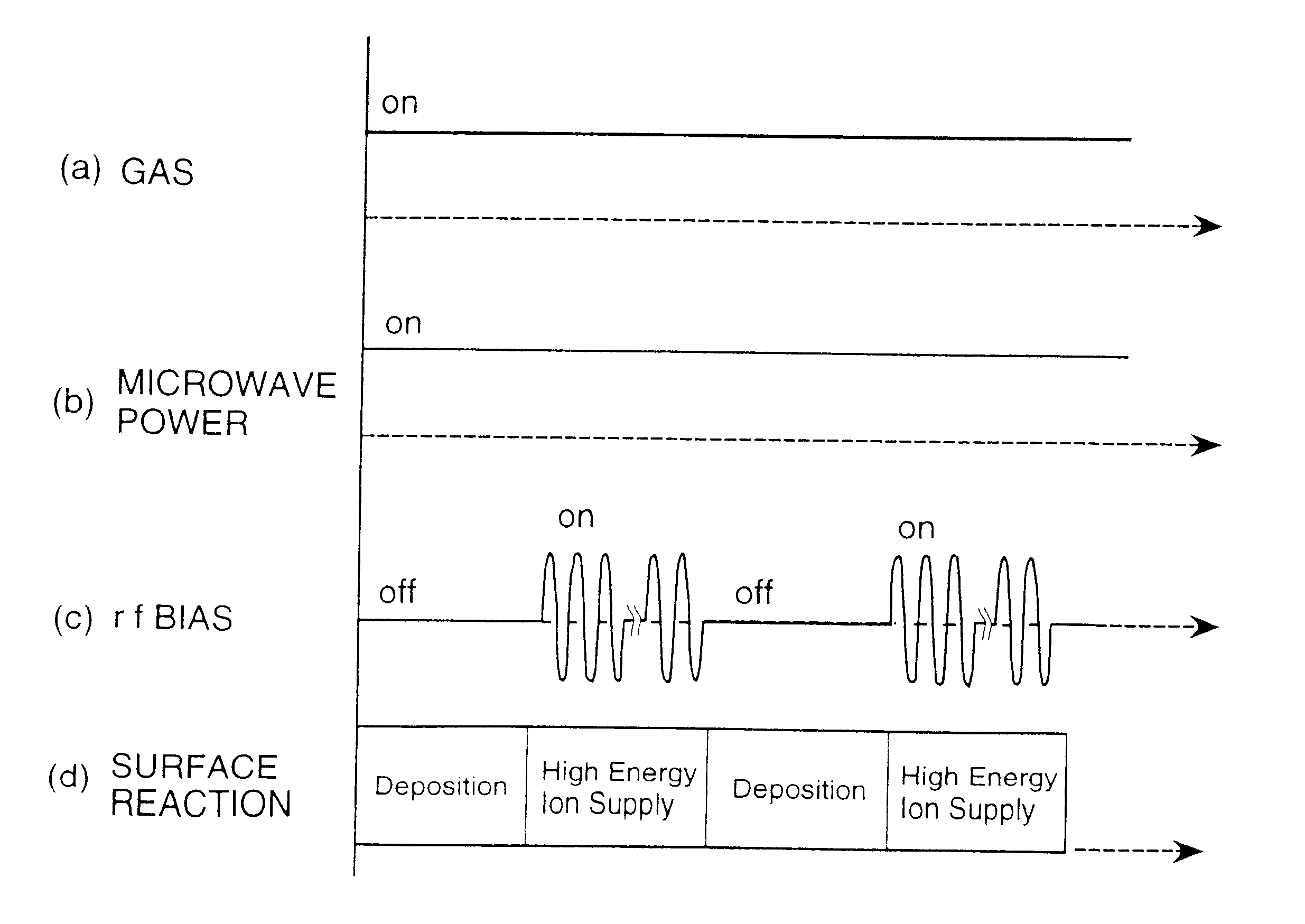
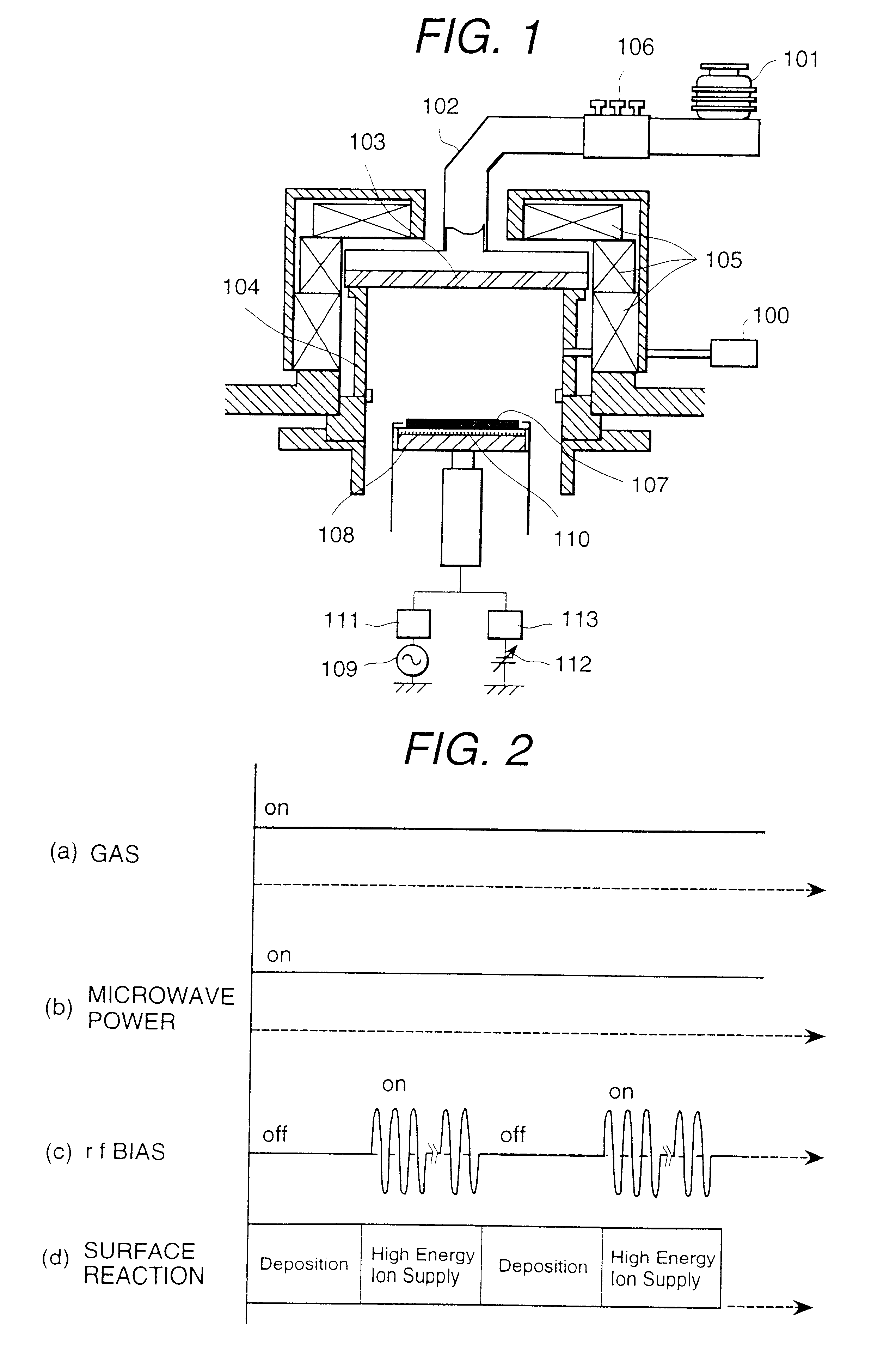
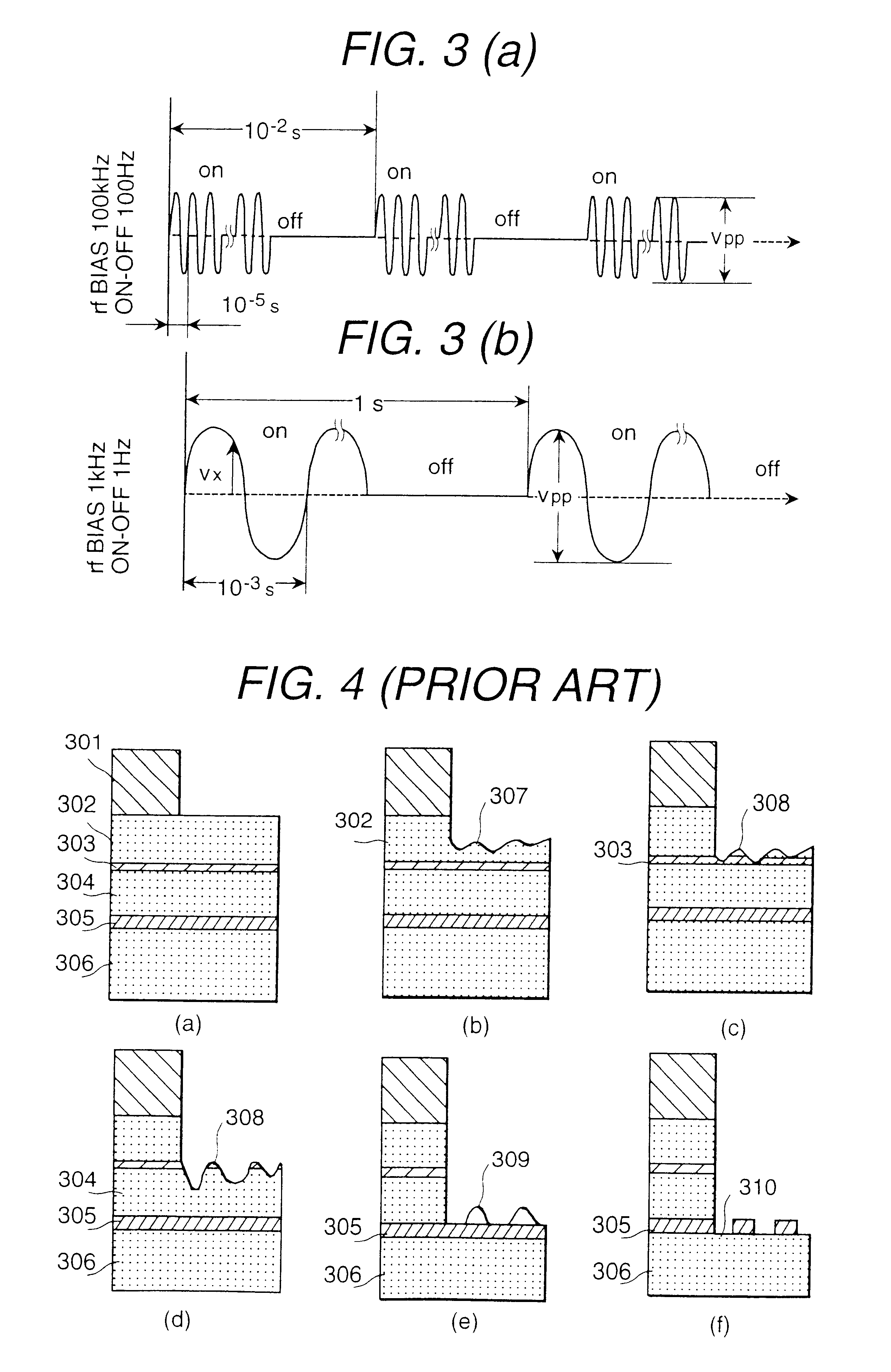
The first description relates to an example of etching a polysilicon metal gate. FIG. 4 shows the temporal change of the cross section of the sample provided with etching treatment according to the conventional method, using the system given in FIG. 1.

FIG. 5 shows the temporal change of the cross sectional profile of the sample processed under the etching conditions according to the present embodiment.

As shown in FIGS. 4(a) and 5(a), the sample in the initial state consists of a multilayer film comprising an oxide film 305, polycrystalline silicon 304, tungsten nitride 303 and tungsten 302 deposited on the silicon substrate 306, with a mask 301 processed to a desired pattern on the top layer. Gas used for etching in this case consists of 30 cc of chlorine and 15 cc of oxygen at a pressure of 0.2 Pa with 500 watts of microwave power at a sample temperature of 70 degrees Celsius.

The conventional example given in FIG. 4 represents the cross section of the sample when etching is perform...

second embodiment

The following describes an embodiment where etching process is divided into several steps in order to increase the effects of said Embodiment:

This embodiment is to get the optimum etching profile by changing the etching conditions at the time point when film type is switched, based on the intensity of light emitted from the plasma during etching or etching time.

Let us take an example of the sample having an architecture shown in FIG. 5. Upon completion of etching of the tungsten 302 and tungsten nitride 303, the condition is selected to allow polycrystalline silicon 304 to be etched to the oxide film 305 at a high selectivity. Namely, since etching of polycrystalline silicon 304 does not require as much ion energy as that in tungsten etching, the radio frequency voltage applied to the sample is reduced. Furthermore, oxygen to accelerates tungsten etching, but it controls etching of polycrystalline silicon, so measures are taken, for example, to select the step where the amount of ox...

third embodiment

The following describes an example of applying the present invention to the etching of the dual gate in comparison with the conventional method:

FIGS. 7(a) and 8(a) are initial cross sectional views representing a sample processed by a system given in FIG. 1. Oxide film 305, n-type polycrystalline silicon 313 and p-type polycrystalline silicon 314 are formed on the silicon substrate 306 of the sample, with a mask 301 processed to a desired pattern on the top layer. Gas used for etching consists of 55 cc of chlorine and 4 cc of oxygen at a pressure of 0.4 Pa with 400 watts of microwave power.

FIG. 7 shows the temporal change of the etching profile of the sample during continuous application of radio frequency voltage (power 35 W) according to the conventional method. A difference in etching depth 311 occurs between the p- and n-type silicons due to the difference of etching rate. This causes processing of n-type polycrystalline silicon 313 to be completed first, as shown in FIG. 7(c). ...


PUM

PropertyMeasurementUnit
frequencyaaaaaaaaaa
frequencyaaaaaaaaaa
radio frequencyaaaaaaaaaa

Abstract

A surface processing method of a sample having a mask layer that does not contain carbon as a major component formed on a substance to be processed, the substance being a metal, semiconductor and insulator deposited on a silicon substrate, includes the steps of installing the sample on a sample board in a vacuum container, generating a plasma that consists of a mixture of halogen gas and adhesive gas inside the vacuum container, applying a radio frequency bias voltage having a frequency ranging from 200 kHz to 20 MHz on the sample board, and controlling a periodic on-off of the radio frequency bias voltage with an on-off control frequency ranging from 100 Hz to 10 kHz.

Description

FIELD OF TECHNOLOGYThe present invention relates to the semiconductor surface treatment method, particularly to etching of the semiconductor surface using plasma.BACKGROUND OF THE INVENTION AND RELATED ART STATEMENTA device of etching the semiconductor in plasma has been known as a means of treating the semiconductor surface. The following describes the prior art with reference to a device based on the ECR (electron cyclotron resonance) method. This is the method to generate plasma through microwaves in a vacuum container where magnetic field is applied from outside. The magnetic field causes electron to perform cyclotron movement, and this frequency and that of the microwaves are made to resonate with each other, thereby ensuring effective generation of plasma. Radio frequency voltage is applied to the sample in order to accelerate ion incident upon a sample such as a semiconductor device. Halogen gas such as chlorine and fluorine is used as a gas to become plasma.Such a convention...

Claims


Application Information

Patent Timeline
Patent Type & Authority Patents(United States)
IPC IPC(8): H01L21/02H01L21/3213
CPCH01J37/32082H01L21/32139H01L21/32136H01L21/3065
Inventor ONO, TETSUOTOKUNAGA, TAKAFUMIUMEZAWA, TADASHIYOSHIGAI, MOTOHIKOMIZUTANI, TATSUMIKURE, TOKUOKOJIMA, MASAYUKISATO, TAKASHIGOTO, YASUSHI
Owner HITACHI LTD
Why Eureka
Try Eureka