Method of making resonant tunneling diodes and CMOS backend-process-compatible three dimensional (3-D) integration

a technology of resonant tunneling diodes and backend processes, applied in the field of solid-state electronics, can solve the problems of poor performance, difficult integration into mainstream sio2 /sub>complementary metal oxide semiconductor) ic technology, and inability to meet the requirements of process and integration, and achieve simple integration, enhance rtd performance, and maintain process and integration requirements. the effect of ease of fabrication

Inactive Publication Date: 2006-02-21
AGENCY FOR SCI TECH & RES
View PDF5 Cites 107 Cited by
  • Summary
  • Abstract
  • Description
  • Claims
  • Application Information

AI Technical Summary

Benefits of technology

[0013]A third object of the present invention is to provide a method of forming an RTD device that allows flexibility in choosing the mixed and asymmetric barrier materials and electrodes so as to enhance the RTD performance while maintaining process and integration requirements and ease of fabrication.
[0014]A fourth object of the present invention is to provide a method of forming such an RTD device wherein front and back end integration includes simple integration with both active and passive interconnect-level devices such as MIM (metal-insulator-metal) capacitors, interconnect inductors, phase shift memories and random access memories.
[0016]A sixth object of the present invention is to provide a method whereby RTD devices can be formed first and then subsequently integrated with planar CMOS / BJT / SiGe devices, circuits and structures using conventional low temperature bonding processes such as anodic bonding, thermal compression, eutectic bonding, plasma bonding, silicon-to-silicon bonding, silicon dioxide bonding, silicon nitride bonding and polymer bonding.
[0017]A seventh object of the present invention is to provide such a formation and integration method whereby a required device area can be selected so as to meet the desired performance parameters of connected devices and circuits.
[0018]An eighth object of the present invention is to provide such a method of forming integrated RTD devices, wherein the devices so formed have good I–V characteristics, such as high peak-to-valley ratio (PVR).
[0022]A twelfth object of the present invention is to provide a method of producing integrated RTD circuits that have small interconnect delays when the RTDs and other associated circuit devices are bonded and electrically connected using Cu—Cu pads.

Problems solved by technology

Although RTDs have been known and used in demonstrating the operation of an oscillator, an amplifier and a mixer at extremely high frequencies and with high resonant current density and very low noise, while maintaining the minimum total device counts and standby current desirable in integrated circuit (IC) technology, they have been difficult to integrate into mainstream Si CMOS (Complementary Metal Oxide Semiconductor) IC technology.
SiO2 is not the only material suitable for the barrier layer that has a wider band gap than silicon.
This is a result of their poor performance, which is due mainly to the large band offset between SiO2 and Si and the excessive thickness of the SiO2 of the buried oxide layer in a silicon-on-insulator (SOI) substrate.
Okuno, in both (U.S. Pat. No. 5,466,949) and (U.S. Pat. No. 5,616,515) discloses a resonant tunneling diode formed by layering silicon dioxide barrier layers on either side of a germanium well, but, as already noted, this device structure is not compatible with silicon processing schemes.

Method used


Image

  • Method of making resonant tunneling diodes and CMOS backend-process-compatible three dimensional (3-D) integration
  • Method of making resonant tunneling diodes and CMOS backend-process-compatible three dimensional (3-D) integration
  • Method of making resonant tunneling diodes and CMOS backend-process-compatible three dimensional (3-D) integration

Examples


first embodiment

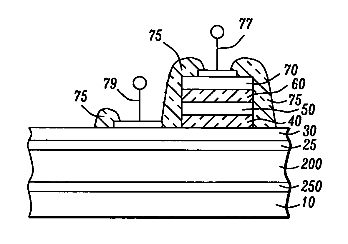
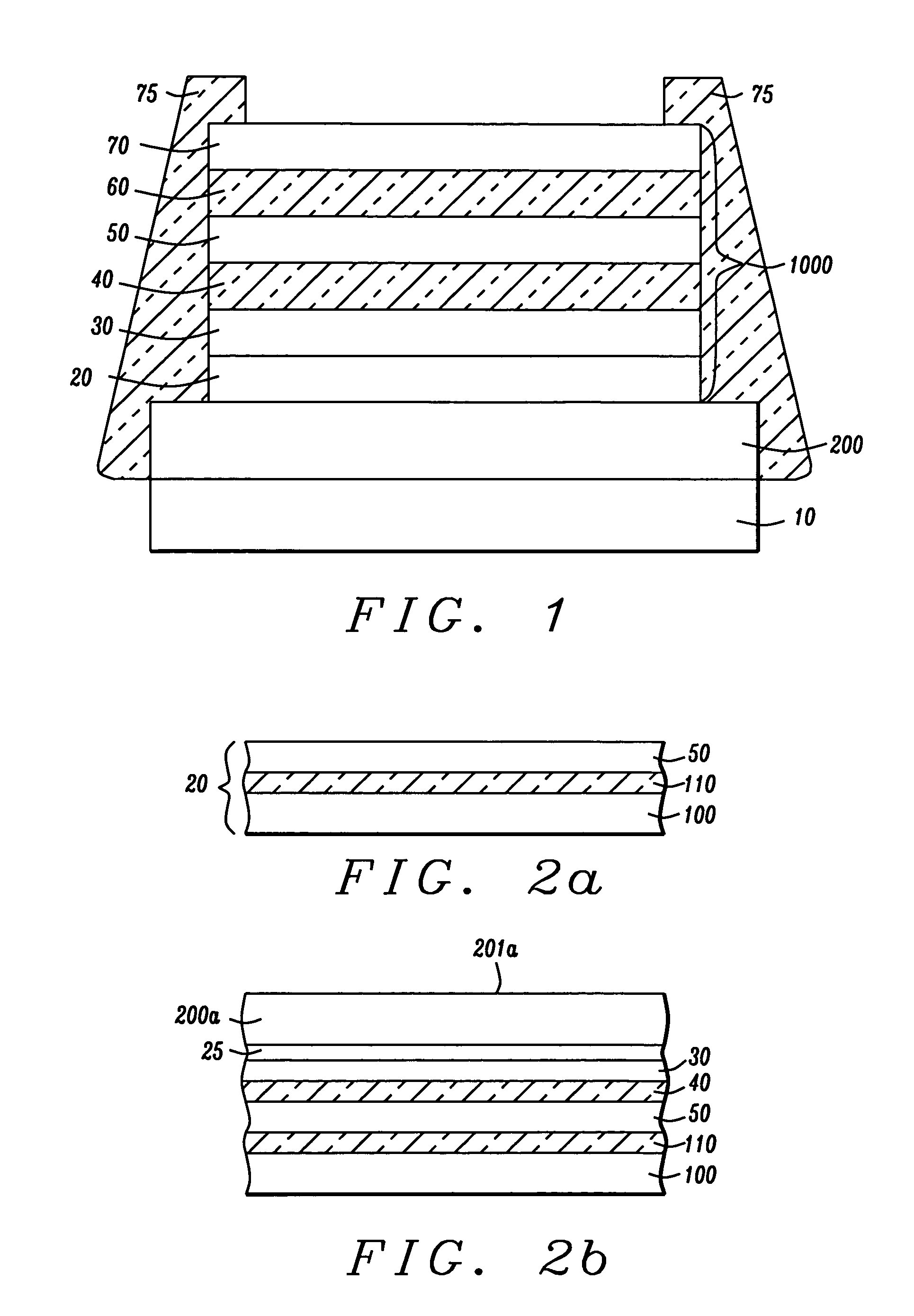
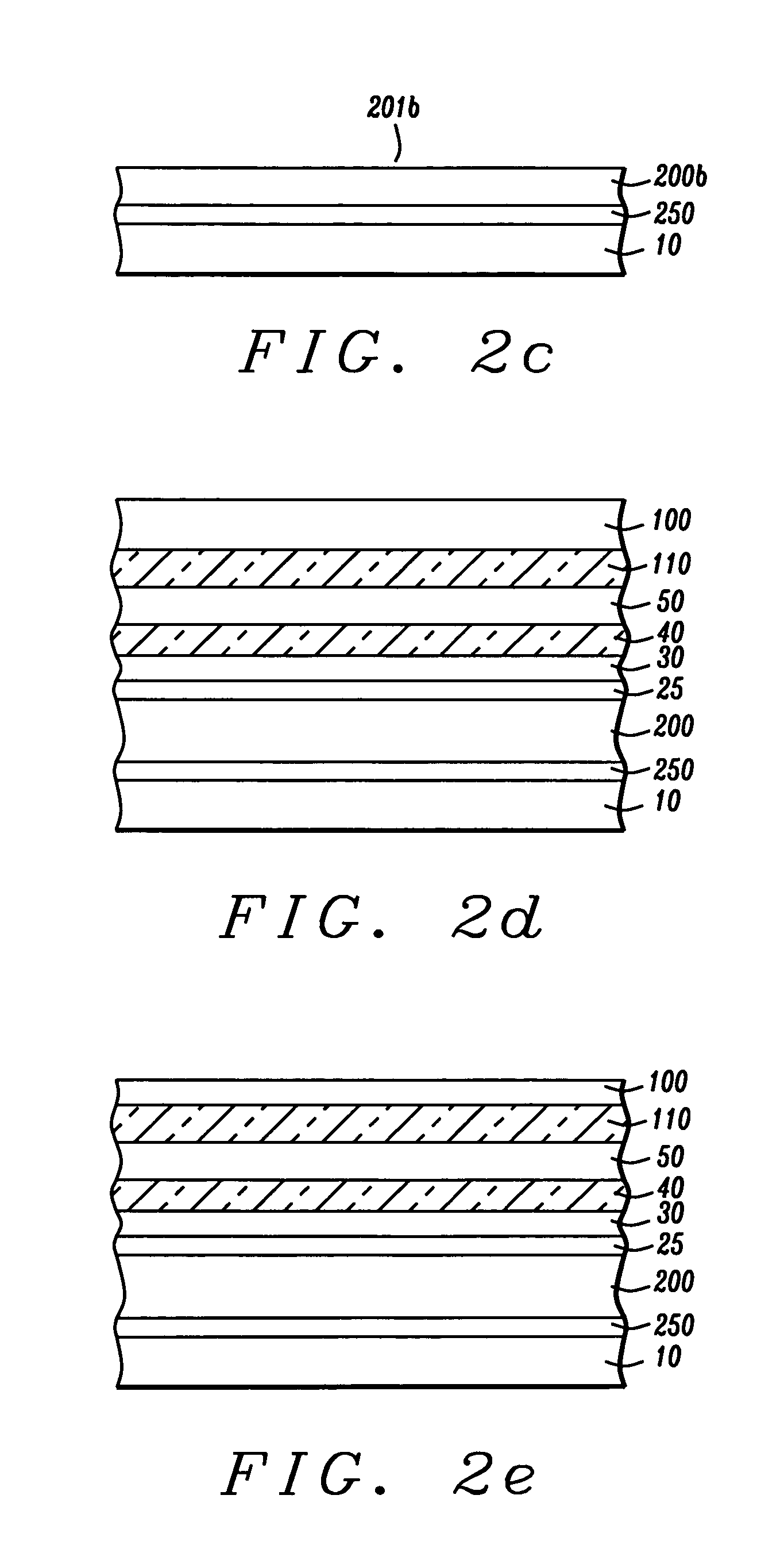
[0034]Referring to FIG. 2a, there is shown an initial process step in a first embodiment that utilizes a semiconductor-on-insulator wafer as the substrate for the RTD fabrication. Within the method of the invention, the wafer can be a Si on insulator (SOI), a Ge on insulator (GOI) or a SiGe on insulator (SiGe—OI) wafer, depending on the nature of the quantum well that is desired. Within the present embodiment a SOi wafer is used as a substrate, but the choice should not be construed as a limitation on the generality of the invention.

[0035]As is well known in the art, the SOI substrate (20) is a tri-layer including a lower Si layer (100), on which is formed a layer of insulating material (110), typically SiO2, which is also called a buried oxide or “BOX” layer, on which is formed an upper layer (50) of monocrystalline silicon (the SOI layer). The upper layer, which will become the quantum well layer, has been reduced in thickness, by an etching process such as oxidation or chemical m...

second embodiment

[0046]the present invention is fabricated using a SOI wafer as in the previous embodiment and applying what is denoted the “smart-cut” technique (a cleavage technique known in the art) to laterally cleave its upper Si layer, then thin it further so that it can be used as a Si well.

[0047]Referring to FIG. 3a, there is shown the first step in this fabrication method in which an upper Si layer (50) of a SOI wafer (20) is implanted through an upper surface (55) with hydrogen to a depth that is less than 100 nm. The implant is represented as shaded region (57). It is noted that the implanted hydrogen, when combined with appropriate subsequent thermal processing of the wafer, produces a lateral cleavage of the upper Si layer (50) (hence the term, “smart-cut”) allowing the lower portion of the layer and the remainder of the SOI substrate beneath it to be removed. It is not the purpose of this invention to describe the smart-cut process, only to indicate that it is a known method of produci...


PUM

PropertyMeasurementUnit
thicknessaaaaaaaaaa
thicknessaaaaaaaaaa
thicknessaaaaaaaaaa

Abstract

A double barrier resonant tunneling diode (RTD) is formed and integrated with a level of CMOS / BJT / SiGe devices and circuits through processes such as metal-to-metal thermocompressional bonding, anodic bonding, eutectic bonding, plasma bonding, silicon-to-silicon bonding, silicon dioxide bonding, silicon nitride bonding and polymer bonding or plasma bonding. The electrical connections are made using conducting interconnects aligned during the bonding process. The resulting circuitry has a three-dimensional architecture. The tunneling barrier layers of the RTD are formed of high-K dielectric materials such as SiO2, Si3N4, Al2O3, Y2O3, Ta2O5, TiO2, HfO2, Pr2O3, ZrO2, or their alloys and laminates, having higher band-gaps than the material forming the quantum well, which includes Si, Ge or SiGe. The inherently fast operational speed of the RTD, combined with the 3-D integrated architecture that reduces interconnect delays, will produce ultra-fast circuits with low noise characteristics.

Description

RELATED APPLICATION[0001]This application is related to previously filed application Ser. No. 10 / 767,275 Filing Date: Jan. 29, 2004 that is assigned to the same assignee as the present application.BACKGROUND OF THE INVENTION[0002]1. Field of the Invention[0003]This invention relates to solid state electronics, in particular to a novel high frequency silicon based resonant tunnel diode with negative differential resistance.[0004]2. Description of the Related Art[0005]The tunnel diode formed by a heavily doped p-n junction was invented by Esaki in 1958. This diode operated on the basis of interband tunneling, wherein charge carriers moved between valence and conduction bands by tunneling through an intervening potential barrier. Subsequently, in 1974, Esaki and co-workers demonstrated a resonant tunneling diode (RTD) consisting of two potential barriers separated by a potential well using a III–V compound semiconductor (L. L Chang, L. Esaki, and R. Tsu, “Resonant tunneling in the semi...

Claims


Application Information

Patent Timeline
Patent Type & Authority Patents(United States)
IPC IPC(8): H01L29/06
CPCB82Y10/00H01L29/882H01L29/66219
Inventor SINGH, JAGARHOU, YONG TIANLI, MING FU
Owner AGENCY FOR SCI TECH & RES
Why Eureka
Try Eureka