

Polyimide film and laminate having metal layer and same
a technology of polyimide film and laminate, which is applied in the field of polyimide film, can solve the problems of misalignment between copper foil pattern and circuit pattern, and dimensional change of laminate, and achieves low coefficient of linear expansion, high modulus of elasticity, and low coefficient of hygroscopic expansion.
- Summary
- Abstract
- Description
- Claims
- Application Information
AI Technical Summary
Benefits of technology
Problems solved by technology
Method used
Image

Examples
first embodiment
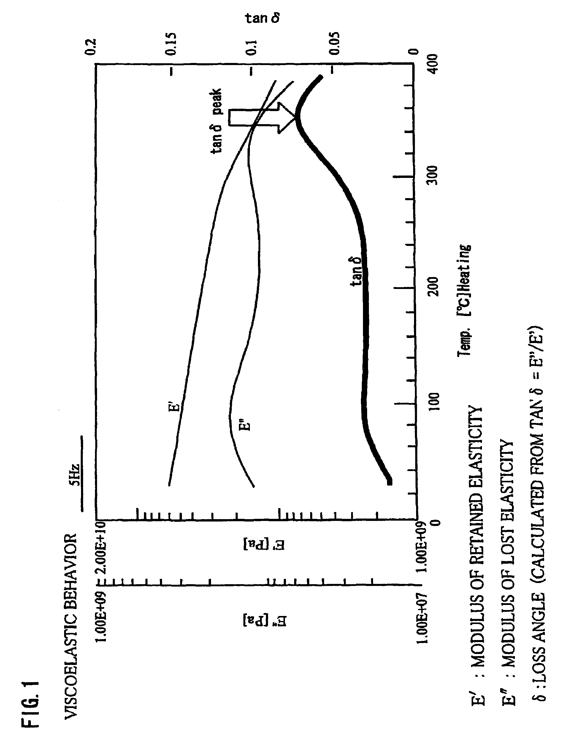
[0059]A first embodiment describes a first polyimide film of the present invention.
[0060]Recently there is a demand for a polyimide film having a low thermal shrinkage rate at a high temperature (300° C.), for preventing imperfect connecting in wiring due to heat that is applied in mounting a precision electric apparatus, such as an IC and an LSI, directly on a polyimide film wired board. Thus, for the present invention, in order to attain a polyimide film having a small thermal shrinkage ratio, intensive studies have been carried out, focusing on a relationship between (a) the thermal shrinkage of the film at a temperature of 300° C. and (b) tan δ peak and tan δ value at 300° C. of dynamic viscoelasticity of the polyimide film. As a result of the intensive studies, it is found that a desirably small thermal shrinkage at the temperature of 300° C. can be attained by arranged such that the tan δ peak of dynamic viscoelasticity of the polyimide film is located in a range of not less t...
second embodiment
[0157]A second embodiment discusses a second polyimide film of the present invention.
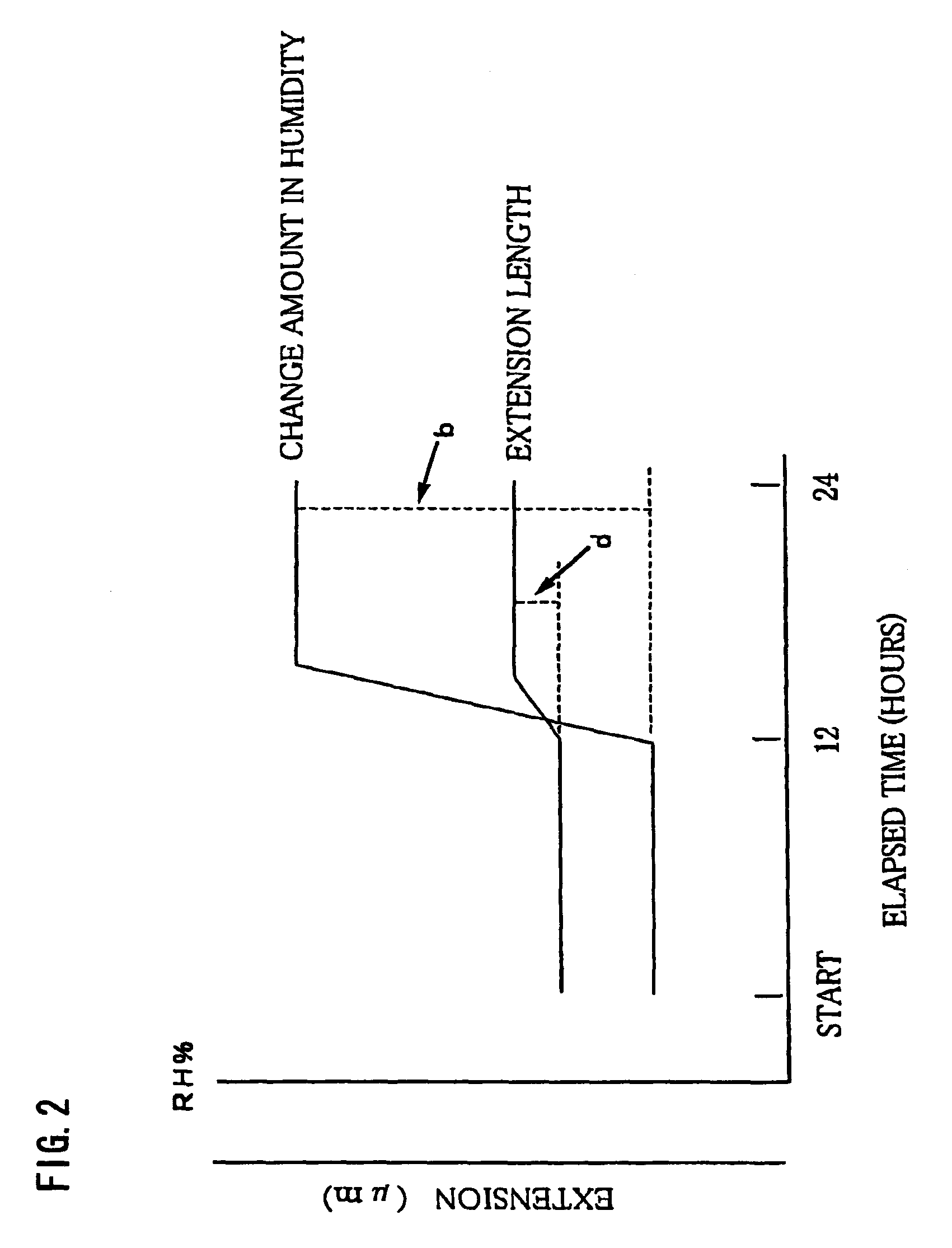
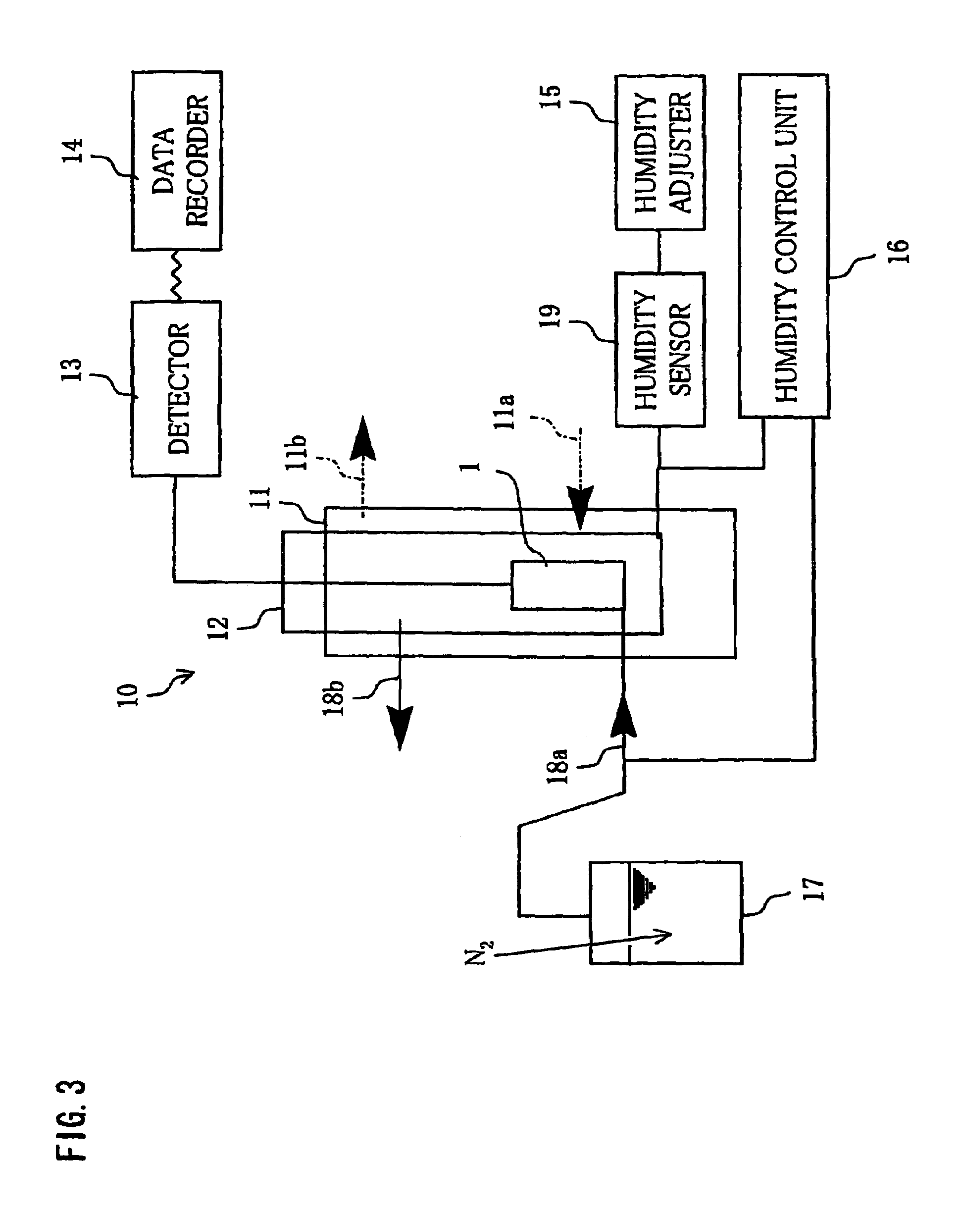
[0158]Conventionally, there is such a problem that long-term stability against harsh environments cannot be attained in a polyimide film that is so suitable for alkali etching that one side thereof can be etched with a 1N potassium hydroxide solution at an etching speed of 0.1 μm / minute (one side) or higher. It is not exactly known why such polyimide film is poor in long-term stability against harsh environments. However, it is considered that hydrolysis causes both of (a) dissolution in alkali-etching the polyimide film and (b) film deterioration caused in harsh environment (the film deterioration being tested in harsh environmental resistance test that tests the stability of the film against harsh environment), especially, in environment of high temperatures and high humidity. That is, the film suitable for the alkali etching is not stable against harsh environment. As a result, it is considered t...
example 1
[0251]In the present example, polyamic acid was produced by using a reactor provided with (i) a stainless separable flask as a reaction vessel, (ii) a stirring screw having two puddles (two-blade stirrer) as a stirring apparatus provided inside the separable flask, and (iii) a cooling apparatus having a cooling capacity of 20.9 kJ / min. In order to prevent water from being mixed in the polymerization, polymerization was carried in a nitrogen gas flowing through the reactor at a rate of 0.05 L / min, the nitrogen gas being dehydrated (desiccated) by passing through silica gel before being introduced into the reactor.
[0252]Into the separable flask, 501.3 g of N,N-dimethyl formamide (DMF) was poured as a polymerization solvent. Then, 25.0 g of 4,4-diaminodiphenyl ether (ODA) and 13.5 g of paraphenylene diamine (p-PDA) were added in the separable flask. Mixture thereof was stirred at a temperature of 20° C., so as to prepare a diamine solution in which ODA and p-PDA were completely dissolv...
PUM
| Property | Measurement | Unit |
|---|---|---|
| Temperature | aaaaa | aaaaa |
| Temperature | aaaaa | aaaaa |
| Temperature | aaaaa | aaaaa |
Abstract
Description
Claims
Application Information