Preparation method of active radical with surface-enhanced Raman scattering (SERS) effect

A surface-enhanced Raman and active substrate technology, applied in Raman scattering, material excitation analysis, etc., can solve problems such as affecting substrate application, poor experimental repeatability and spectral reproducibility, and inability to obtain metal particles with surface roughness.

Inactive Publication Date: 2012-10-31
BEIJING UNIV OF CHEM TECH
View PDF9 Cites 52 Cited by
  • Summary
  • Abstract
  • Description
  • Claims
  • Application Information

AI Technical Summary

Problems solved by technology

However, the active substrate obtained by these methods has a single structure, and metal particles with a high surface roughness cannot be obtained, which limits the enhancement effect of the SERS active substrate on the Raman signal. In addition, the experimental repeatability and spectral reproducibility are poor, which affects the substrate in molecular Applications in the detection field

Method used


Image

  • Preparation method of active radical with surface-enhanced Raman scattering (SERS) effect

Examples


Embodiment 1

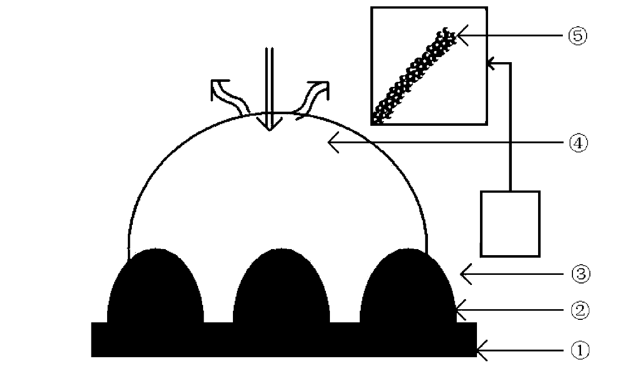
[0026] 1. Add 40mL of 0.5mol / L hydrofluoric acid into a 50mL autoclave, weigh 0.162g ferric nitrate and mix hydrofluoric acid to make an etching solution, and polish the p-type (111) silicon with a resistivity of 0.01-0.09 Ωcm on one side The slices were cut into square slices with a size of 2 cm × 2 cm, put into an autoclave, and etched at 170° C. for 5 minutes to obtain nano-silicon.

[0027] 2. Put 0.2g of zinc powder into the tubular heating furnace, use a gas flow meter to feed 20 sccm oxygen as a reaction gas, and 80 sccm nitrogen as a protective gas, and use a vacuum pump to control the pressure of the reaction chamber at about 5 Torr. The obtained nano-silicon was placed downstream of the zinc source gas flow, and reacted at 400° C. for 60 minutes to obtain a zinc oxide nanowire array.

[0028] 3. Prepare a mixed solution of 0.1mM chloroauric acid and 0.1mM methanol, soak the nanowire structure substrate prepared by steps 1 and 2 in the solution, and react at 100°C for...

Embodiment 2

[0032] 1. Add 80mL of 7mol / L hydrofluoric acid solution into a 100ml autoclave, weigh 3.23g of ferric nitrate and dissolve it in the hydrofluoric acid solution. Cut single-sided polished n-type (100), resistivity 30-50Ωcm monocrystalline silicon wafer into 2cm×2cm size, and fix it in etching solution. Corrosion at 70° C. for 100 minutes to obtain a silicon nanoporous pillar array.

[0033] 2. Add 0.5g of titanium dioxide powder to the hydrothermal reaction kettle, and add 40mL of 0.1M sodium hydroxide solution. The nano-silicon substrate prepared by the above method is placed in the solution, and the reaction kettle is heated to 140° C. in a vacuum drying oven and kept for 20 minutes. After cooling to room temperature, the substrate was taken out, washed with deionized water and alcohol, and dried to obtain a silicon-based titania nanowire array.

[0034] 3. Prepare 0.01M silver nitrate solution and 0.01M sodium borohydride ethanol solution, soak the substrate prepared under...

Embodiment 3

[0038] 1. Add 40ml of saturated hydrofluoric acid solution and 40ml of absolute ethanol into a 100ml beaker as the electrolyte. Single-sided polished n-type (111) single-crystal silicon wafers with a resistivity of 5-10 Ω cm were cut into a size of 2 cm × 2 cm, cleaned and fixed in an etching solution. A carbon rod is used as a cathode, and a current of 300 mA is passed through, and the silicon nanoporous column array is obtained by etching for 10 min.

[0039] 2. Put 0.5g zinc powder into the tubular heating furnace, utilize gas flowmeter to feed 20sccm oxygen as reaction gas, 600sccm nitrogen as protective gas, utilize vacuum pump to control reaction chamber pressure at about 50 Torr, the obtained in step 1 Nano-silicon is placed near the upstream of the zinc source gas flow, and reacted at 900° C. for 10 minutes to obtain a zinc oxide nanowire array.

[0040] 3. Prepare 0.1M silver nitrate solution and 0.1M sodium borohydride ethanol solution, soak the substrate prepared u...


PUM

PropertyMeasurementUnit
diameteraaaaaaaaaa

Abstract

The invention provides a preparation method of an active radical with a surface-enhanced Raman scattering (SERS) effect, belongs to the technical field of spectrum detection, and relates to the preparation technology of the SERS active radical, which is rapid, has high sensitivity and performs a low trace detection function. The preparation method is characterized in that firstly, a nano porous silicon columnar array with a large specific surface area is prepared by utilizing a hydrothermal etching technology; afterwards, a nanowire structure of an II-VI group compound semiconductor (such as zinc oxide, titanium dioxide, cadmium sulfide, cadmium selenide, cadmium telluride, and the like) by utilizing a chemical vapor deposition method; and finally, nano particles of precious metal (such as gold, silver, copper and the like) are finally prepared on the nanowire structure by using a chemical reduction method, so as to obtain an active radical material. The preparation method has a wide application prospect in the aspects of clinical biomolecular fast recognition, trace chemical substance detection, biological sample analysis, and the like. The preparation method has the advantages that the preparation process of each material is simple, the condition is mild and the repetition rate reaches 100 percent.

Description

Technical field: [0001] The invention belongs to the technical field of Raman spectrum detection, and in particular relates to a method for preparing a metal / compound semiconductor nanowire active substrate with multiple structures and based on a surface-enhanced Raman scattering effect. This method is simple and easy to implement, and has high repeatability. The prepared sensor substrate has the characteristics of high sensitivity, fast detection speed and wide applicability. For example, the active substrate of the sensor can be applied to rapid trace detection of residual pesticide molecules in food, Whether there are harmful substances such as bisphenol A in the raw materials of infant feeding bottles, or whether there are excessive polychlorinated biphenyls and other toxic and harmful substances in the tap water. The on-site rapid detection of toxic and harmful substances, especially trace substances, realized by the present invention is an applied technology that is urge...

Claims


Application Information

Patent Timeline
Patent Type & Authority Applications(China)
IPC IPC(8): G01N21/65
Inventor 许海军廛宇飞苏雷张常兴孙晓明
Owner BEIJING UNIV OF CHEM TECH
Why Eureka
Try Eureka