X-ray detector based on nano carbon material/silicon heterojunction and preparation method thereof

A nano-carbon material, silicon heterojunction technology, used in X-ray detectors and their preparation, X-ray detectors, X-ray detection fields, can solve problems such as poor X-ray transmittance, poor sensitivity, and device dead layer thickness. , to achieve the effect of preventing transmission, high transmission rate, and improving response rate

Active Publication Date: 2018-12-28
CHINA ACADEMY OF SPACE TECHNOLOGY
View PDF4 Cites 0 Cited by
  • Summary
  • Abstract
  • Description
  • Claims
  • Application Information

AI Technical Summary

Problems solved by technology

However, there are also some problems in the current semiconductor detectors. For example, due to the small band gap of the germanium material in the high-purity germanium detector, in order to suppress the dark current, the detector often needs to be cooled; the window layer of the gold-silicon surface barrier detector Gold is used, and gold, being a heavy metal (atomic number 79), is poorly transparent to X-rays
For example, the X-ray transmittance of 250nm gold to 1keV photon energy is less than 5%, which seriously affects the detection efficiency of the detector; the silicon PIN detector needs to use thermal diffusion and other technologies in the preparation process, and the dead layer of the device is relatively high. Thick and therefore less sensitive to lower energy X-ray detection

Method used


Image

  • X-ray detector based on nano carbon material/silicon heterojunction and preparation method thereof
  • X-ray detector based on nano carbon material/silicon heterojunction and preparation method thereof
  • X-ray detector based on nano carbon material/silicon heterojunction and preparation method thereof

Examples


Embodiment 1

[0041] (1) Single-walled carbon nanotubes were prepared by chemical vapor deposition. Through purification and spreading, a thin film with a thickness of 250nm was obtained;

[0042] (2) transferring the single-walled carbon nanotube film to one side surface of the N-type silicon wafer, and drying in a natural state;

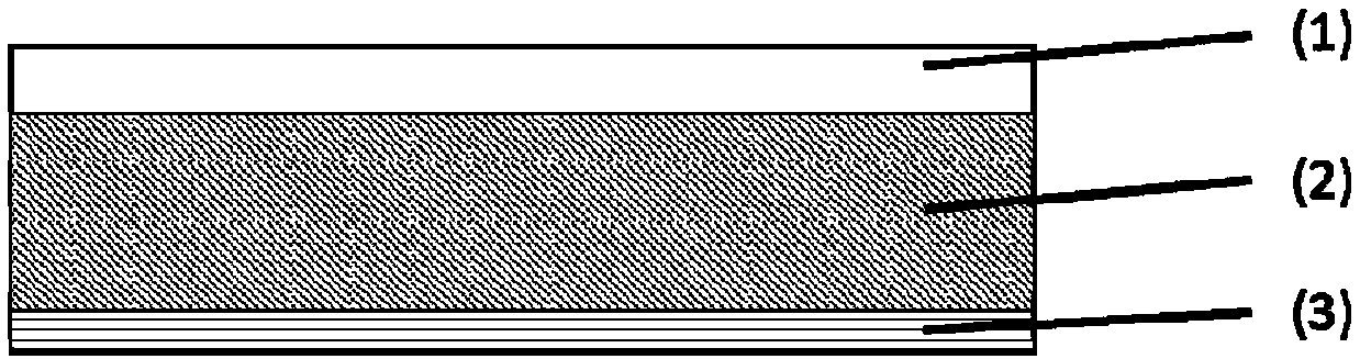
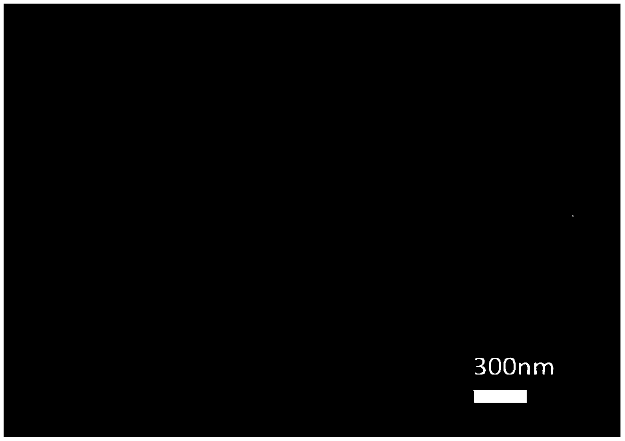
[0043] (3) Ti / Au metal electrode of 50nm is vapor-deposited on the other side of silicon wafer, thereby obtains carbon nanotube / silicon heterojunction X-ray detector, and its structure is as follows figure 1 shown. figure 2 Shown is a scanning electron micrograph of the carbon nanotube film in the detector;

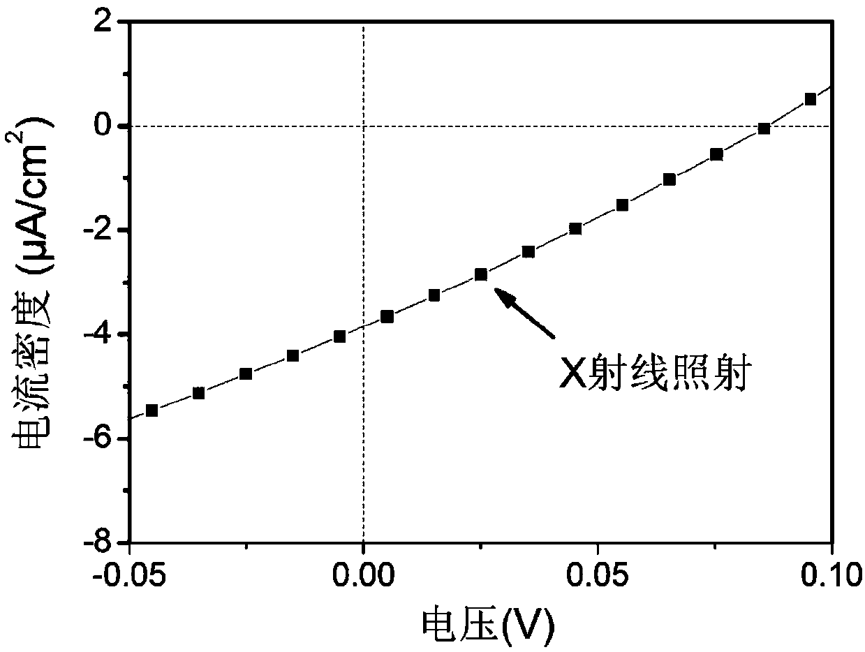
[0044] (4) The detector is at 6.5mGy air Under the irradiation of X-rays / s, the current-voltage characteristic curve of the device is as follows image 3 As shown, its short-circuit current density reaches 3.85μA / cm 2 , while the short-circuit current density of the gold-silicon surface barrier detector as a control sample is only 2.5μA / cm 2 , the res...

Embodiment 2

[0047] (1) Graphene was prepared on nickel foil by chemical vapor deposition. Corroding the nickel substrate with ferric chloride solution to obtain a graphene film with a thickness of 1 μm;

[0048] (2) Transfer the graphene film to one side surface of the N-type silicon chip, and dry it under the irradiation of an infrared oven lamp;

[0049] (3) Coating an indium-gallium alloy on the other side of the silicon wafer as a lower electrode to obtain a graphene / silicon heterojunction X-ray detector. Figure 5 Shown is a scanning electron micrograph of the graphene film in the detector.

[0050] (4) The detector is at 4mGy air / s of X-ray irradiation, the current-voltage characteristic curve of the device is as follows Image 6 As shown, its short-circuit current density reaches 2.16μA / cm 2 , which is higher than the short-circuit current density of the gold-silicon surface barrier detector of the control sample under the same test conditions (only 1.57μA / cm 2 ), the respons...

Embodiment 3

[0052] (1) Multi-walled carbon nanotubes were prepared by chemical vapor deposition. Through purification and spreading, a film with a thickness of 10 μm was obtained;

[0053] (2) The multi-walled carbon nanotube film is transferred to one side surface of the N-type silicon wafer, and blown dry by nitrogen;

[0054] (3) Coating 100nm indium gallium alloy on the other side of the silicon wafer as the bottom electrode, so as to obtain a carbon nanotube / silicon heterojunction X-ray detector.

[0055] (4) The detector is at 2mGy air / s of X-ray irradiation, the current-voltage characteristic curve of the device shows that its short-circuit current density reaches 1.15μA / cm 2 , while the short-circuit current density of the gold-silicon surface barrier detector as a control sample is only 0.79μA / cm 2 , the response of the device of the present invention is 45.6% higher than that of the control sample.


PUM

PropertyMeasurementUnit
thicknessaaaaaaaaaa
thicknessaaaaaaaaaa

Abstract

An X-ray detector based on nano carbon material/silicon heterojunction of the present invention uses nano carbon material and silicon to form a heterojunction, and the nano carbon material is used asa transparent window layer of X-rays and an upper electrode of a device. The nano-carbon material is composed of carbon element with atomic number 6. At the same thickness, the X-ray transmittance ofthe material is much higher than that of the traditional gold material (atomic number 79). For example, the X-ray transmittance of 250nm carbon nano-material is 95%, and that of 250nm gold nano-material is less than 5% for 1keV photon energy. That is, under the same irradiation conditions, the detector of the invention can be used for ionizing electron holes in silicon, and the effective number ofX-ray photons for generating electric signals will be much larger than that of the conventional gold-silicon surface barrier detector, so that the response rate of the detector can be greatly improved.

Description

technical field [0001] The invention relates to an X-ray detector, in particular to an X-ray detector based on a nano-carbon material / silicon heterojunction and a preparation method thereof, belonging to the technical field of nano-carbon material application, and the detector described in the invention can be used for X-ray detection in high-energy physics, astrophysics, industry, safety inspection, nuclear medicine, X-ray imaging, military and other fields. Background technique [0002] X-rays are electromagnetic waves with a wavelength between ultraviolet rays and gamma rays, and their wavelengths are very short, ranging from 0.01 to 100 Angstroms. X-rays have high penetrating power and can penetrate many substances that are opaque to visible light. They have important applications in high-energy physics, astrophysics, industry, safety testing, nuclear medicine, X-ray imaging, military and other fields. [0003] An X-ray detector is a device that converts X-rays into ele...

Claims


Application Information

Patent Timeline
Patent Type & Authority Applications(China)
IPC IPC(8): H01L31/0224H01L31/028H01L31/118H01L31/18B82Y30/00
CPCB82Y30/00H01L31/022408H01L31/028H01L31/1185H01L31/1804Y02P70/50
Inventor 贾怡郭楠肖林刘军库
Owner CHINA ACADEMY OF SPACE TECHNOLOGY
Why Eureka
Try Eureka