Alkali etching and polishing method for monocrystalline silicon wafer

A monocrystalline silicon wafer, alkali etching technology, applied in the direction of polishing composition containing abrasives, chemical instruments and methods, preparation of organic compounds, etc., can solve the increasingly high requirements for silicon wafers of solar cells Problems such as reflectivity and etching and polishing loss need to be improved to achieve good etching and polishing effects, improved photoelectric conversion efficiency, and low thinning

Active Publication Date: 2022-01-28
绍兴拓邦新能源股份有限公司
View PDF22 Cites 2 Cited by
  • Summary
  • Abstract
  • Description
  • Claims
  • Application Information

AI Technical Summary

Problems solved by technology

However, the current alkali etching and polishing method for monocrystalline silicon wafers still has many defects, such as the surface reflectivity of silicon wafers, etching and polishing losses, etc., which still need to be improved. With the development of solar cell technology, the requirements for solar cell silicon wafers Higher and higher

Method used


Image

  • Alkali etching and polishing method for monocrystalline silicon wafer
  • Alkali etching and polishing method for monocrystalline silicon wafer
  • Alkali etching and polishing method for monocrystalline silicon wafer

Examples


Embodiment 1

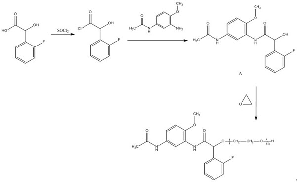
[0066] This embodiment provides a fluorine-containing nonionic surfactant, which is specifically prepared by the following method:

[0067] 1) Add 20.4 parts by weight of D-o-fluoromandelic acid to 60 parts by weight of dichloromethane, add 0.2 parts by weight of tetrabutylammonium halide, stir evenly, add 17.8 parts by weight of thionyl chloride, and stir at 115°C for reaction 8h, normal pressure distillation, obtain 21.2gD-o-fluoromandeloyl chloride, the molar yield is 93.9%;

[0068] 2) 18.1 parts by weight of 3-amino-4-methoxyacetanilide, the D-o-fluoromandelic acid chloride prepared in step 1) are added to 40 parts by weight of methylene chloride, and 0.08 parts by weight of 4-aminopyridine is added. Adjust the pH to 9.6 with sodium hydroxide solution, stir and react at room temperature for 12 hours, evaporate the solvent under reduced pressure, extract the residue with dichloromethane, wash with hydrochloric acid and deionized water in turn to obtain 30.5 g of product A,...

Embodiment 2

[0072] This embodiment provides an alkali etching and polishing method for a single crystal silicon wafer, comprising the following steps:

[0073] 1) Surface pretreatment: use 10wt% hydrofluoric acid solution to pretreat the monocrystalline silicon wafer to remove the phosphosilicate glass layer on the back;

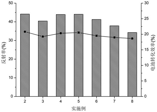
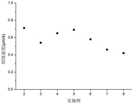
[0074] 2) Surface etching and polishing: 8 parts by weight of lanthanum oxide (with a particle size of 50 nm, the same below), 0.6 parts by weight of glycerin, 0.3 parts by weight of sodium tartrate, 1 part by weight of 2-methylaminoethanol, and 0.4 parts by weight of the product prepared in Example 1 The obtained fluorine-containing nonionic surfactant and 89.7 parts by weight of deionized water were evenly mixed to obtain a polishing solution, and the back of the silicon chip was etched and polished at a temperature of 50° C. for 8 minutes. Microwave treatment was used to assist in the polishing process; microwave The processed power is 300W;

[0075] 3) Surface clea...

Embodiment 3

[0080] This embodiment provides another alkali etching and polishing method for a single crystal silicon wafer. The only difference from Example 2 is that the polishing liquid consists of 8 parts by weight of lanthanum oxide, 0.6 parts by weight of glycerin, 0.16 parts by weight of sodium tartrate, 1 It is prepared by mixing parts by weight of 2-methylaminoethanol, 0.4 parts by weight of the fluorine-containing nonionic surfactant prepared in Example 1, and 89.84 parts by weight of deionized water.


PUM


Abstract

The invention provides an alkali etching and polishing method for a monocrystalline silicon wafer and belongs to the technical field of silicon wafer etching. According to the method, an alkaline polishing solution containing grinding particles, glycerol, an organic amine compound, sodium tartrate, a fluorine-containing nonionic surfactant and sodium tartrate is utilized to perform etching and polishing on monocrystalline silicon through the steps of surface pretreatment, surface etching and polishing, alkali cleaning, acid cleaning, water washing and the like, etching and polishing at the low temperature are achieved, energy consumption is reduced, the etching and polishing effect is good, the silicon wafer thinning amount is low, and the silicon wafer surface reflectivity and the battery conversion efficiency are effectively improved.

Description

technical field [0001] The invention relates to the technical field of silicon wafer etching, in particular to an alkali etching and polishing method for single crystal silicon wafers. Background technique [0002] The etching and polishing process is a crucial step in the solar cell production process. Etching and polishing are divided into dry etching and wet etching, in which wet etching is acid etching using an acidic solution of mixed acids such as hydrofluoric acid, nitric acid, and acetic acid, or using sodium hydroxide or potassium hydroxide, etc. Alkaline solution for alkali etching. Acid etching can control the etching rate, and the surface morphology of the wafer after etching is good, but the etching rate of acid etching is too fast, which leads to the degradation of the flatness of the wafer; compared with acid etching, the etching rate of alkali etching is low, However, alkali etching can improve the flatness of the wafer, so a wafer with excellent flatness c...

Claims


Application Information

Patent Timeline
Patent Type & Authority Applications(China)
IPC IPC(8): C09G1/02C09K23/42C09K23/22C07C231/12C07C231/14C07C235/52C08G65/28H01L21/02H01L21/306H01L31/18
CPCC09G1/02H01L31/1804H01L21/30604H01L21/02057C07C231/14C07C231/12C08G65/2633C08G65/2612C07C235/38C07C235/52
Inventor 李一鸣吴冰张震华
Owner 绍兴拓邦新能源股份有限公司
Why Eureka
Try Eureka