Method for forming thin semiconductor film, method for fabricating semiconductor device, system for executing these methods and electrooptic device

a technology of thin semiconductor film and system, applied in the field of thin semiconductor film, can solve the problems of increasing the cost of the apparatus with scaling up, achieving the attainable limit of carrier mobility of about 80 to 120, and difficult to obtain a crystal having a grain diameter of 500 nm or mor

Inactive Publication Date: 2003-08-07
SONY CORP
View PDF2 Cites 172 Cited by
  • Summary
  • Abstract
  • Description
  • Claims
  • Application Information

AI Technical Summary

Benefits of technology

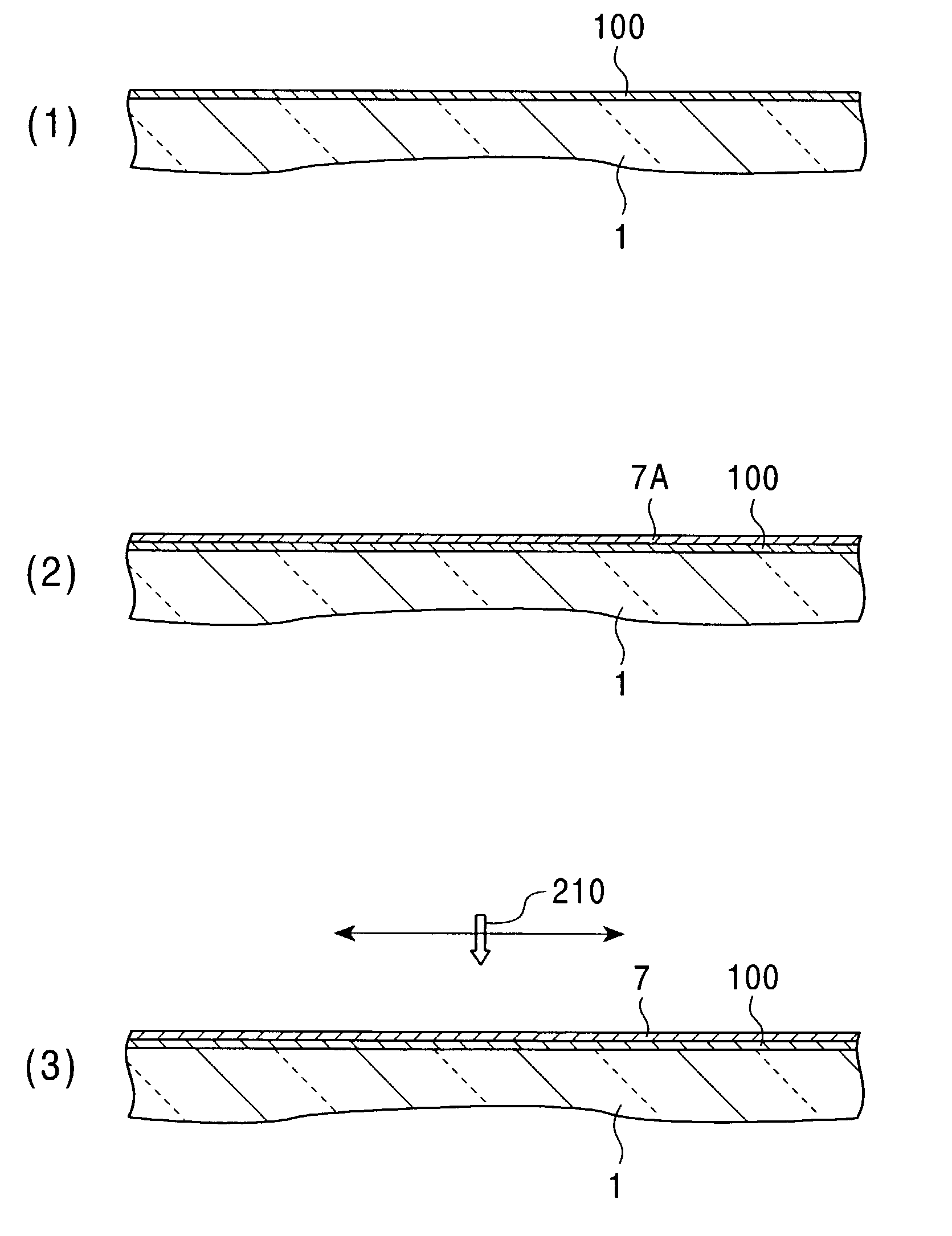
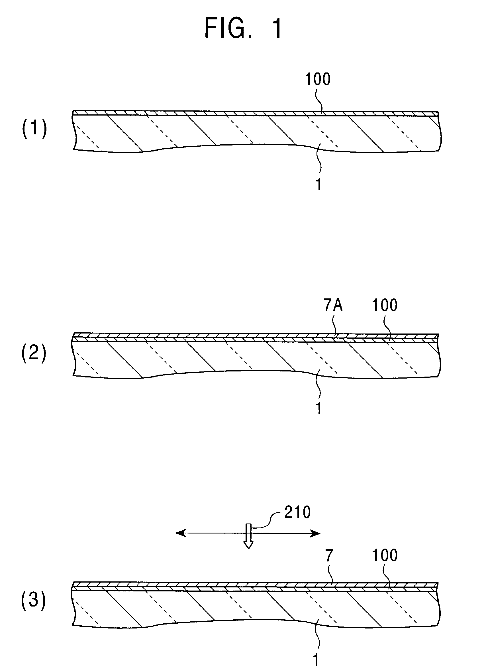
[0015] In the present invention, a low-crystalline semiconductor thin film is formed on the substrate, and heated in a molten state, a semi-molten state or non-molten state by annealing with UV or / and DUV laser (referred to as "laser annealing of the present invention" or "the above-described laser annealing" hereinafter) formed by optical harmonic generation using the non-linear optical effect and cooled to promote crystallization of the low-crystalline semiconductor thin film, forming a polycrystalline or monocrystalline semiconductor thin film. Therefore, the following remarked effects (1) to (12) can be obtained.
[0288] (k) Since optical harmonic modulated UV or / and DUV laser annealing can be performed at a low temperature (200 to 400.degree. C.), low-strain-point glass and a heat-resistant resin, which are inexpensive and can easily realize a large size, can be used, thereby decreasing the weight and cost.

Problems solved by technology

However, this method has an attainable limit of carrier mobility of about 80 to 120 cm.sup.2 / V.multidot.sec.
Therefore, even in a method sufficiently removing hydrogen and oxygen, which inhibit crystal growth, by heating the substrate to a temperature of about 400.degree. C. to control the solidification speed, it is difficult to obtain a crystal having a grain diameter of 500 nm or more.
However, there are a lot of the problems of instability of excimer laser output, productivity, an increase in apparatus cost with scaling up, deterioration in yield and quality, etc.
Particularly, in a large glass substrate of 1 m.times.1 m, the problems are made significant to cause further difficulties in improving performance and quality and decreasing the cost.
However, this method causes the catalytic element to remain in the formed crystalline silicon film.
However, the process is complicated, the gettering effect is insufficient, and the semiconductor properties of the silicon film deteriorate to deteriorate stability and reliability of an element formed.
Therefore, the limit of the substrate size is a wafer size of 8 to 12 inches .phi., and expensive quartz glass having high heat resistance must be used, causing difficulties in decreasing the cost, and limiting application to EVF and a data / AV projector.
In the catalytic CVD method, a carrier mobility of about 30 cm.sup.2 / V.multidot.sec can be obtained without crystallization annealing, but a good MOSTFT device cannot be sufficiently formed.
Furthermore, when the polycrystalline silicon film is formed on the glass substrate, a transition layer (thickness of 5 to 10 nm) of initial amorphous silicon is readily formed depending upon the deposition conditions, and desired carrier mobility cannot easily be obtained in a bottom gate MOSTFT.
In a LCD using a polycrystalline silicon MOSTFT and integrated with a driving circuit, in general, bottom gate MOSTFTs can easily be produced from the viewpoint of yield and productivity, but the problem of difficulty in obtaining desired carrier mobility is a bottleneck.

Method used


Image

  • Method for forming thin semiconductor film, method for fabricating semiconductor device, system for executing these methods and electrooptic device
  • Method for forming thin semiconductor film, method for fabricating semiconductor device, system for executing these methods and electrooptic device
  • Method for forming thin semiconductor film, method for fabricating semiconductor device, system for executing these methods and electrooptic device

Examples


first embodiment

[0356] As described above, in this embodiment, like in the first embodiment, V.sub.th can easily be controlled with high carrier mobility in the gate channel, source and drain regions of the MOSTFTs in the display section and the peripheral driving circuit section of the LCD by the vapor phase growth such as catalytic CVD or plasma CVD and laser annealing of the present invention, and a polycrystalline silicon film with low resistance and a high operation speed can be formed. A liquid crystal display device using the top gate-, bottom gate- or dual gate-type MOSTFT formed by the polycrystalline silicon film can be formed in a structure in which the LDD structure display section with high switching property and low leakage current is integrated with the peripheral circuits such as a high-performance driving circuit, a video signal processing circuit, a memory, etc., thereby permitting the realization of an inexpensive liquid crystal panel with high image quality, high definition, a n...

third embodiment

[0377] In this embodiment, the present invention is applied to an organic or inorganic electroluminescence (EL) display device, for example, an organic EL display device. An example of the structure and an example of manufacture of the organic EL display device are described below. Although, in this embodiment, the top gate-type MOSTFT is used as an example, the bottom gate-type or dual gate-type MOSTFT may be used.

[0378]

[0379] As shown in FIGS. 31(A) and (B), in Example I of the structure, gate channel regions 117, source regions 120 and drain regions 121 of switching MOSTFT 1 and current driving MOSTFT 2 are formed by using a polycrystalline silicon film (or a monocrystalline silicon film) with high crystallinity and a large grain diameter. (Although the polycrystalline silicon film is described below as an example, the monocrystalline silicon film can be used in the same manner.) Also, gate electrodes 115 are formed on a gate insulating film 118, and source electrodes 127 and dr...

fourth embodiment

[0428] In this embodiment, the present invention is applied to a field emission display device (FED). Examples the structure and manufacture of this display device are described below. Although, in this embodiment, a top gate-type MOSTFT is described as an example, bottom gate-type and dual gate-type MOSTFTs may be used as described above.

[0429]

[0430] As shown in FIGS. 35(A), (B) and (C), in Example I of the structure, gate channel regions 117, source regions 120 and drain regions 121 of switching MOSTFTs 1 and current driving MOSTFTs 2 are formed on a glass substrate 111 by the above-described method based on the present invention using a polycrystalline silicon film having high crystallinity and a large grain diameter. Also, gate electrodes 115 are formed on a gate insulating film 118, and source electrodes 127 and drain electrodes 128 are formed on the source and drain regions. The drain of the MOSTFT 1 and the gate of the MOSTFT 2 are connected through the drain electrode 128, ...


PUM

PropertyMeasurementUnit
carrier mobilityaaaaaaaaaa
electron mobilityaaaaaaaaaa
grain diameteraaaaaaaaaa

Abstract

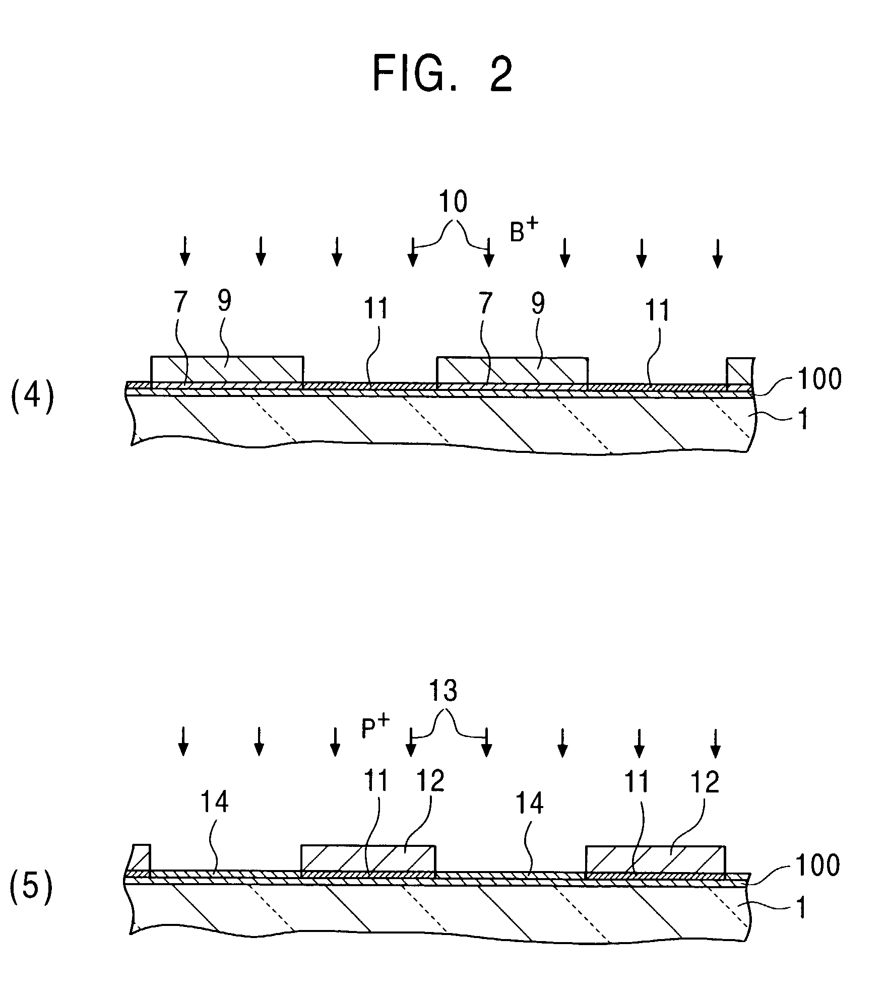
The present invention provides a method capable of easily forming a polycrystalline or monocrystalline semiconductor thin film of polycrystalline silicon with a high degree of crystallization and high quality at low cost, and an apparatus for carrying out the method. In a method of forming a polycrystalline (or monocrystalline) semiconductor thin film, a method of manufacturing a semiconductor device and an apparatus for carrying out these methods, in order to form a large-grain polycrystalline (or monocrystalline) semiconductor thin film (7) such as a polycrystalline silicon film with a high degree of crystallization on a substrate (1) or manufacturing a semiconductor device having the polycrystalline (or monocrystalline) semiconductor thin film (7), a low-crystalline semiconductor thin film (7A) is formed on the substrate (1), and then heated in a molten, semi-molten or non-molten state by laser annealing with ultraviolet rays (UV) or / and deep ultraviolet rays (DUV) and cooled to promote crystallization of the low-crystalline semiconductor thin film (7A), obtaining the polycrystalline (or monocrystalline) semiconductor thin film (7).

Description

[0001] The present invention relates to a method and apparatus for forming a polycrystalline semiconductor thin film of polycrystalline silicon on a substrate by laser annealing or the like, a method and apparatus for manufacturing a semiconductor device having the polycrystalline semiconductor thin film formed on the substrate, and an electrooptic device.[0002] In a MOSFET (Metal-Oxide-Semiconductor Field Effect Transistor), for example, a MOSTFT (Thin Film Transistor=thin film gate-type field effect transistor), source, drain and channel regions are conventionally formed by a vapor growth method such as a plasma CVD (CVD: Chemical Vapor Deposition), a low-pressure CVD method, a catalytic CVD method, or the like, a solid growth method, a liquid growth method, an excimer laser annealing method, or the like using a polycrystalline silicon film.[0003] As disclosed in Japanese Unexamined Patent Application Publication No. 7-131030 and 9-116156, and Japanese Examined Patent Application ...

Claims


Application Information

Patent Timeline
Patent Type & Authority Applications(United States)
IPC IPC(8): G02F1/1368B23K26/352G09F9/30H01J9/02H01L21/20H01L21/268H01L21/336H01L27/08H01L27/088H01L27/32H01L29/786H01L31/04H01L31/077H01L31/18
CPCH01L21/2026H01L29/66757H01L29/66765H01L27/1285H01L29/78675H01L29/78678H01L29/78648Y02E10/546H01L21/0262H01L21/02683H01L21/02678H01L21/02502H01L21/02422H01L21/02488H01L21/02532H01L21/02672H01L21/02595H01L21/02691H01L21/02686
Inventor YAMANAKA, HIDEO
Owner SONY CORP
Why Eureka
Try Eureka