Method of manufacturing CMOS devices by the implantation of N- and P-type cluster ions

Inactive Publication Date: 2007-05-10
SEMEQUIP
View PDF17 Cites 12 Cited by
  • Summary
  • Abstract
  • Description
  • Claims
  • Application Information

AI Technical Summary

Benefits of technology

[0016] While it is possible to design beam transport optics which are nearly aberration-free, the ion beam characteristics (spatial extent, spatial uniformity, angular divergence and angular uniformity) are nonetheless largely determined by the emittance properties of the ion source itself (i.e., the beam properties at ion extraction which determine the extent to which the implanter optics can focus and control the beam as emitted from the ion source). The use

Problems solved by technology

Such electron flood systems introduce additional variables into the manufacturing process, and cannot completely eliminate yield losses due to surface charging.
As semiconductor devices become smaller and smaller, transistor operating voltages and gate oxide thicknesses become smaller as well, reducing the damage thresholds in semiconductor device manufacturing, further reducing yield.
Unfortunately, this technology is not yet commercially available, and indeed negative ion implantation has not to the author's knowledge been used to fabricate integrated circuits, even in research and development.
While it is possible to produce semiconductor dopant ions such as boron by this method, the ion currents tend to be low, the beam emittance tends to be large, and the presence of cesium vapor presents a nearly unacceptable risk to wafer yield, since alkaline metals are considered very serious contaminants to silicon processing.
Recently, the ion energy required for many critical implants has decreased to the point that conventional ion implantation systems, which were originally developed to generate much higher energy beams, are not effective at providing the necessary implant.
The limitations of conventional ion implantation systems at low beam energy are most evident in the extraction of ions from the ion source, and th

Method used


Image

  • Method of manufacturing CMOS devices by the implantation of N- and P-type cluster ions
  • Method of manufacturing CMOS devices by the implantation of N- and P-type cluster ions
  • Method of manufacturing CMOS devices by the implantation of N- and P-type cluster ions

Examples


Example

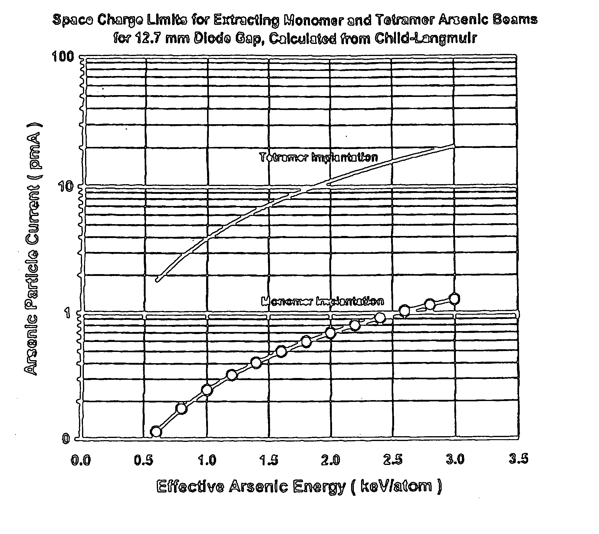
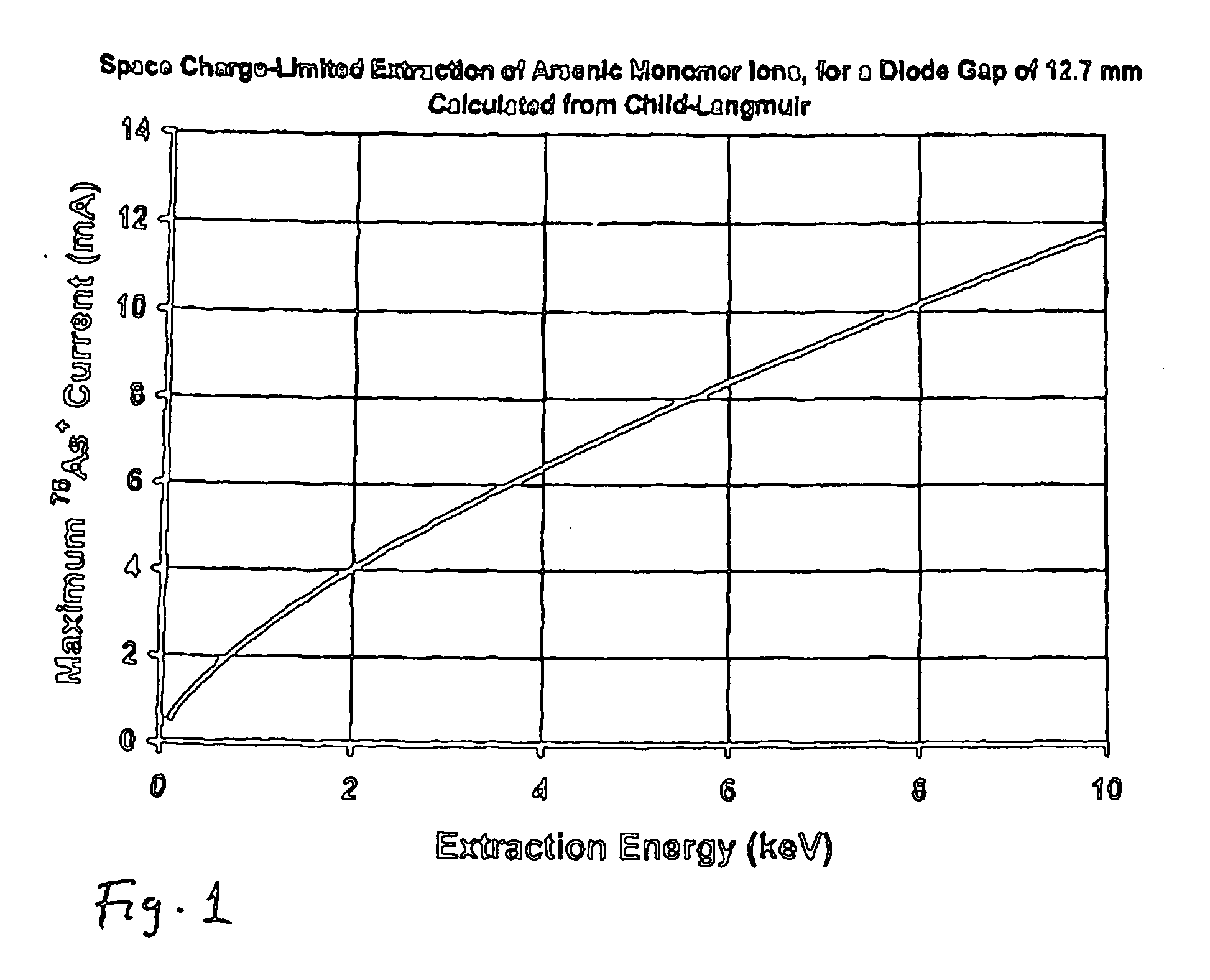
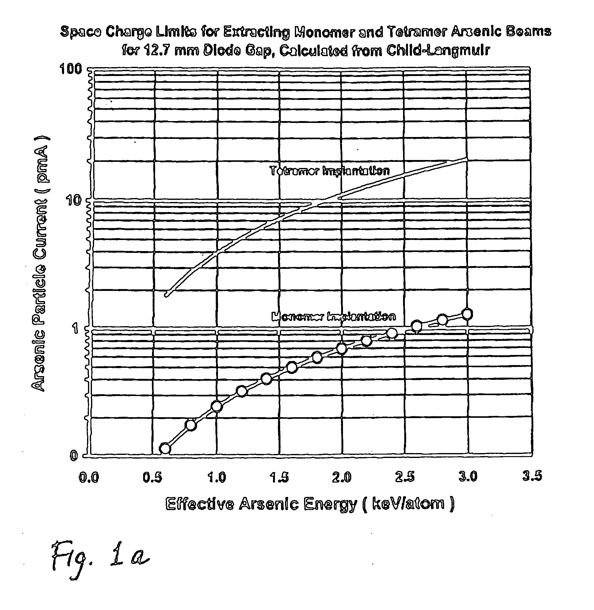
[0052]FIG. 2 is a conceptual diagram of a cluster ion source 10 and its various components. A supply of feed gas 11 is provided, such as a cylinder of AsH3, PH3, B2H6 or vaporized B10H14. The feed material can be stored in a cylinder as a gas at room temperature, or can be introduced as vapor sublimated from a heated solid or evaporated from a liquid phase. The feed gas supply 11 is connected to an ionization chamber 13 through a flow controller 12. The flow controller 12 can be as sophisticated as a computer-controlled mass flow controller, or as simple as a connecting tube with predetermined gas conductance. In the latter case, the flow is varied by controlling the pressure of the gas in 11. The controlled flow of dopant-containing gaseous feed material creates a stable gas pressure within the ionization chamber 13, for example, between approximately 3×10⁻⁴ Torr and 3×10⁻³ Torr. Ionization energy 14 is provided in the form of a controlled current of electrons with a defined energy...


PUM


Abstract

A method of manufacturing a semiconductor device is described, wherein clusters of N- and P-type dopants are implanted to form the transistor structures in CMOS devices. For example, As4Hx+clusters and either B10Hx or B10Hx+ clusters are used as sources of As and B doping, respectively, during the implants. An ion implantation system is described for the implantation of cluster ions into semiconductor substrates for semiconductor device manufacturing. A method of producing higher-order cluster ions of As, P, and B is presented, and a novel electron-impact ion source is described which favors the formation of cluster ions of both positive and negative charge states. The use of cluster ion implantation, and even more so the implantation of negative cluster ions, can significantly reduce or eliminate wafer charging, thus increasing device yields. A method of manufacturing a semiconductor device is further described, comprising the steps of providing a supply of dopant atoms or molecules into an ionization chamber, combining the dopant atoms or molecules into clusters containing a plurality of dopant atoms, ionizing the dopant clusters into dopant cluster ions, extracting and accelerating the dopant cluster ions with an electric field, selecting the desired cluster ion by mass analysis, modifying the final implant energy of the cluster ion through post-analysis ion optics, and implanting the dopant cluster ions into a semiconductor substrate. In general, dopant clusters contain n dopant atoms where n can be 2, 3, 4 or any integer number. This method provides the advantages of increasing the dopant dose rate to n times the implantation current with an equivalent per dopant atom energy of 1/n times the cluster implantation energy. This is an effective method for making shallow transistor junctions, where it is desired to implant with a low energy per dopant atom.

Description

CROSS-REFERENCE TO RELATED APPLICATIONS [0001] This patent application is a continuation-in-part of commonly owned copending U.S. patent application Ser. No. ______, filed on Sep. 16, 2002, entitled Electron Beam Ion Source With Integral Low-Temperature Vaporizer, by Thomas N, Horsky, which is a continuation of U.S. patent application Ser. No. 09 / 736,097, filed on Dec. 13, 2000, now U.S. Pat. No. 6,452,338. This patent application also claims priority of commonly owned copending U.S. provisional patent application Ser. No. 60 / 391,847, filed on Jun. 26, 2002, entitled Doping by the Implantation of Cluster Ions; and commonly owned copending U.S. provisional patent application Ser. No. 60 / 392,271, filed on Jun. 26, 2002, entitled Cluster Beam Ion Implantation Using Negative Ions. [0002] The following patent applications, herein incorporated by reference, are also related to the present application: PCT Application, Ser. No. PCT / US00 / 33786, filed Dec. 13, 2000, entitled “Ion Implantatio...

Claims


Application Information

Patent Timeline
IPC IPC(8): H01L21/8238H01L21/336H01J37/317H01L21/265H01L21/425H01L27/092
CPCH01J2237/31701H01L21/26513H01L21/26566H01L21/823842H01L21/425H01L21/823814H01L21/2658H01L21/265
Inventor HORSKY, THOMAS NEILJACOBSON, DALE CONRADKRULL, WADE ALLEN
Owner SEMEQUIP
Why Eureka
Try Eureka