

Ion implantation device and a method of semiconductor manufacturing by the implantation of ions derived from carborane molecular species
- Summary
- Abstract
- Description
- Claims
- Application Information
AI Technical Summary
Benefits of technology
Problems solved by technology
Method used
Image

Examples
Embodiment Construction
Cluster Ion Implantation System
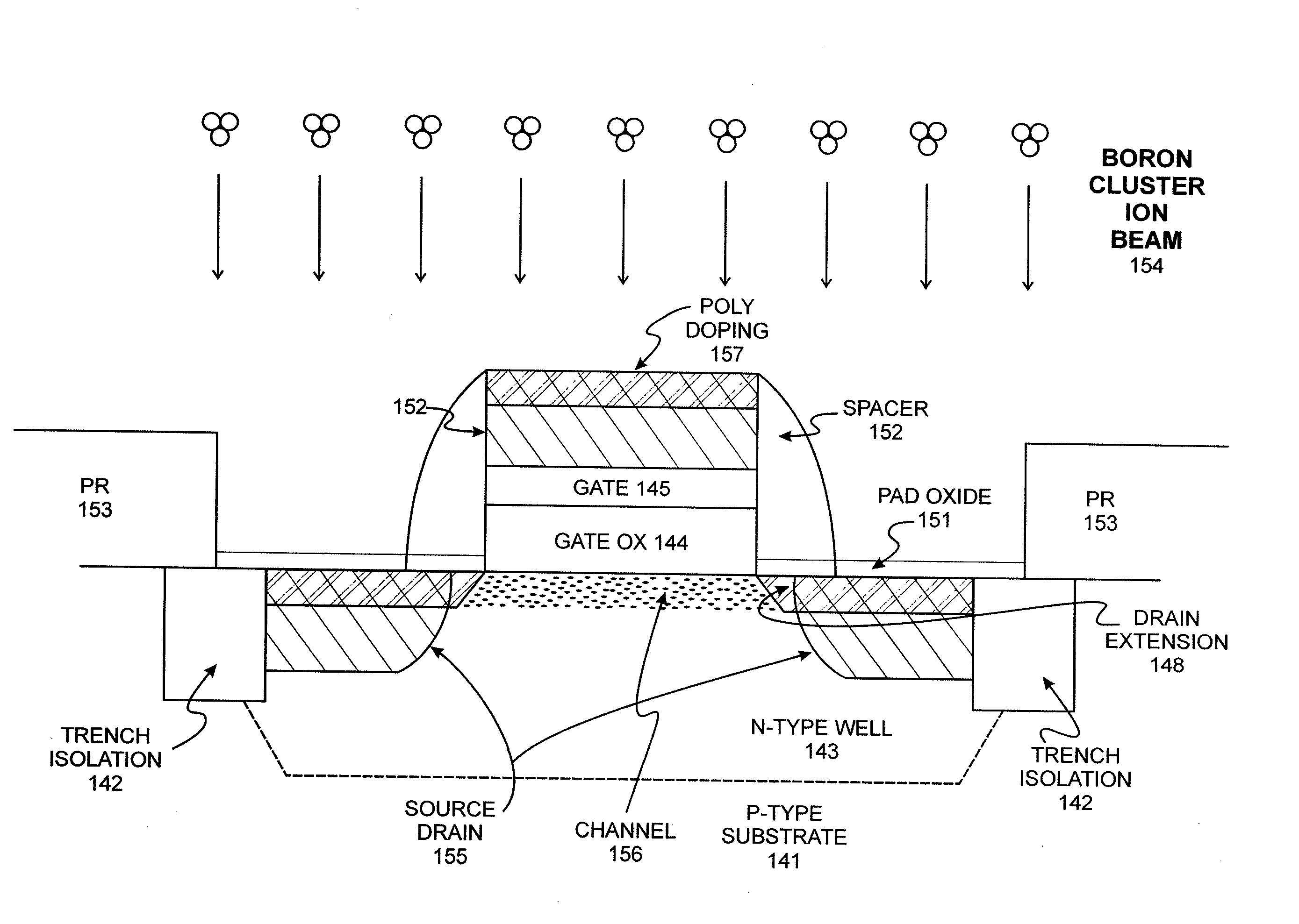
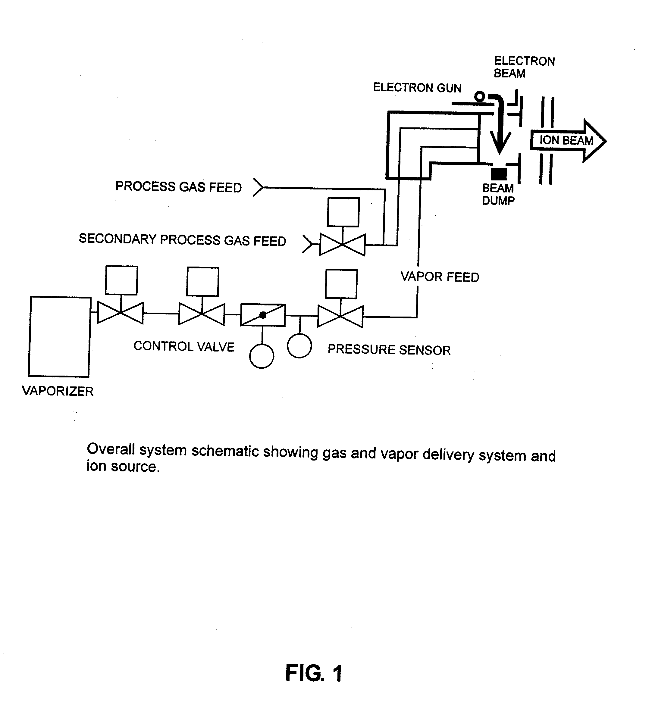
[0039]FIG. 1A is a schematic diagram of a cluster ion implantation system of the high current type for use with the present invention. In particular, the present invention relates to the use of source materials of carborane molecules such as, C2B10H12, C2B8H10 and C4B18H22 that are ionized and used as a dopant material for a semiconductor substrate. Configurations for ion implantation devices other than that shown in FIG. 1A are possible. In general, the electrostatic optics of ion implanters employ slots (apertures displaying a large aspect ratio in one dimension) embedded in electrically conductive plates held at different potentials, which tend to produce ribbon beams, i.e., beams which are extended in one dimension. This approach has proven effective in reducing space-charge forces, and simplifies the ion optics by allowing the separation of focusing elements in the dispersive (short axis) and non-dispersive (long axis) directions. The cluster ion ...
PUM
 Abstract
Description
Claims
Application Information