Gallium trichloride injection scheme

Inactive Publication Date: 2009-07-16
S O I TEC SILICON ON INSULATOR THECHNOLOGIES
View PDF27 Cites 43 Cited by
  • Summary
  • Abstract
  • Description
  • Claims
  • Application Information

AI Technical Summary

Benefits of technology

[0019]Typically, the reaction chamber is made of quartz. Also, the reaction chamber may be surrounded by an enclosure which is operatively associated with one or more fans for circulating air in the enclosure to lower the t

Problems solved by technology

However, their commercial use has been substantially hindered by the lack of readily available single crystal substrates.
It is a practical impossibility to grow bulk single crystal substrates of the Group III-nitride compounds using traditional methods, such as Czochralski, vertical gradient freeze, Bridgeman or float zone, that have been used for other semiconductors such as silicon or GaAs.
While various high pressure techniques have been investigated, they are extremely complicated and have lead to only very small irregular crystals.
The lack of a native single crystal substrate greatly increases the difficulty in making epitaxial Group III-nitride layers with low defect densities and desirable electrical and optical properties.
A further difficulty has been the inability to make p-type GaN with sufficient conductivity for use in practical devices.
Differences in the lattice constant, thermal coefficient of expansion and crystal structure between the III-nitride epitaxial layer and the substrate lead to a high density of defects, stress and cracking of the III-nitride films or the substrate.
Furthermore, sapphire has a very high resistivity (cannot be made conductive) and has poor thermal conductivity.
SiC substrates can be produced in both conductive and highly resistive forms, but is much more expensive than sapphire and only available in smaller diameters (typically 50 mm diameter with 150 mm and 200 mm as demonstrations).
While the use of sapphire and SiC are suitable for some device applications, the high defect density associated with III-nitride layers grown on these substra

Method used


Image

  • Gallium trichloride injection scheme
  • Gallium trichloride injection scheme
  • Gallium trichloride injection scheme

Examples


example

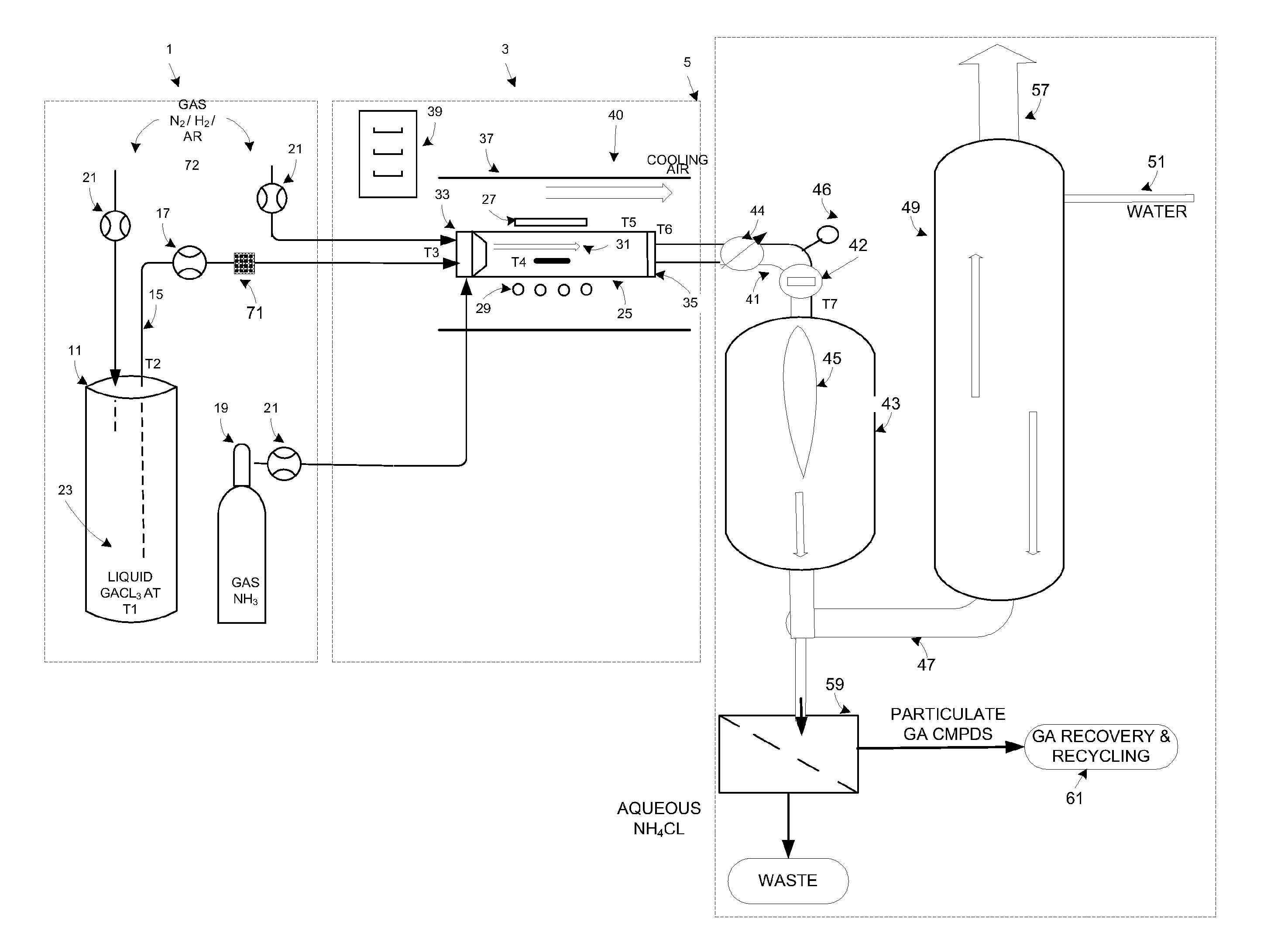
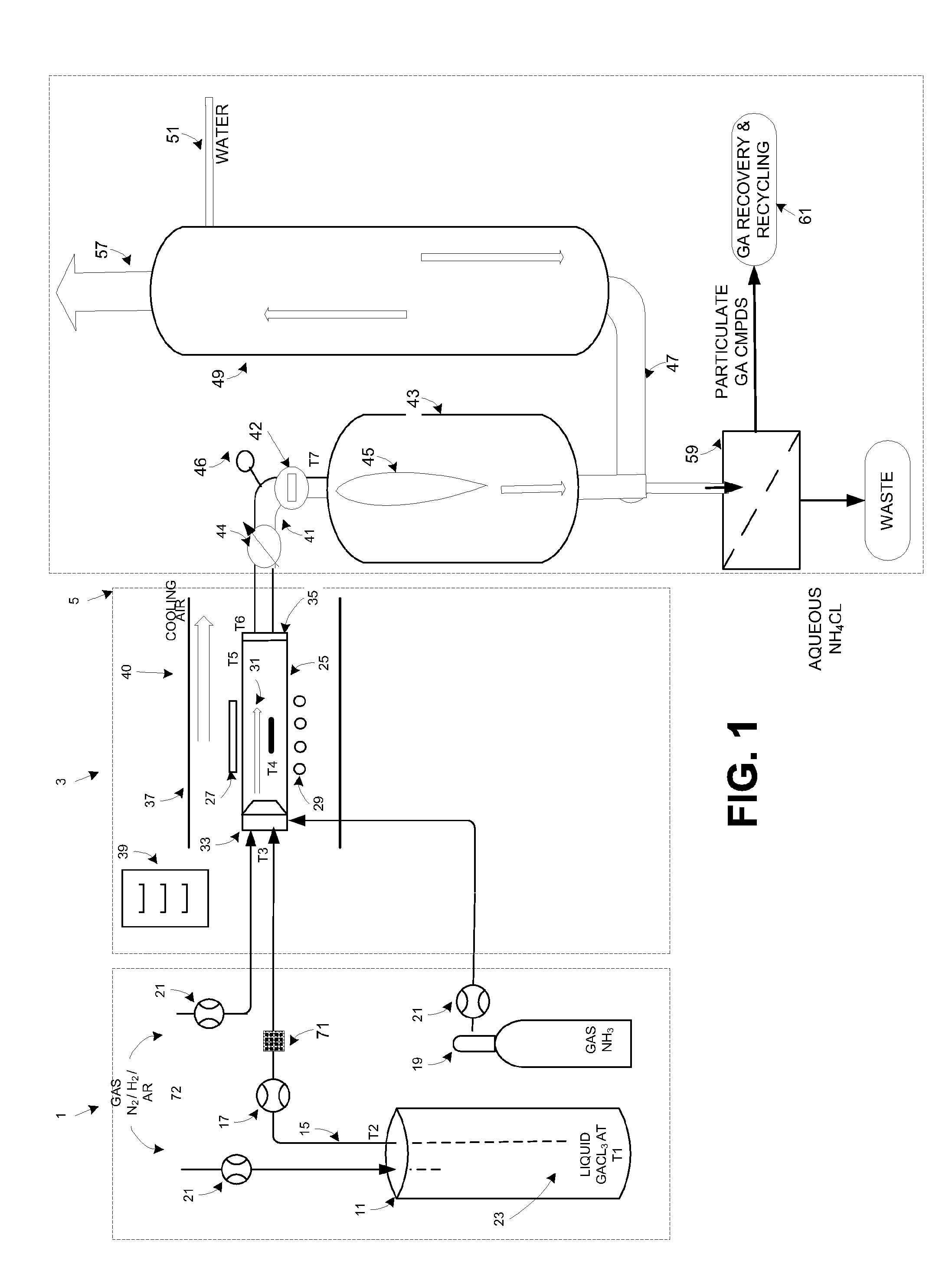
[0120]The invention is now compared to a standard or conventional HVPE system to illustrate the advantages and unexpected benefits that are provided when conducting HVM of Group III-V material according to the invention. Prior to setting forth this comparison and by way of introduction, conventional HVPE systems are first briefly described in relevant part.

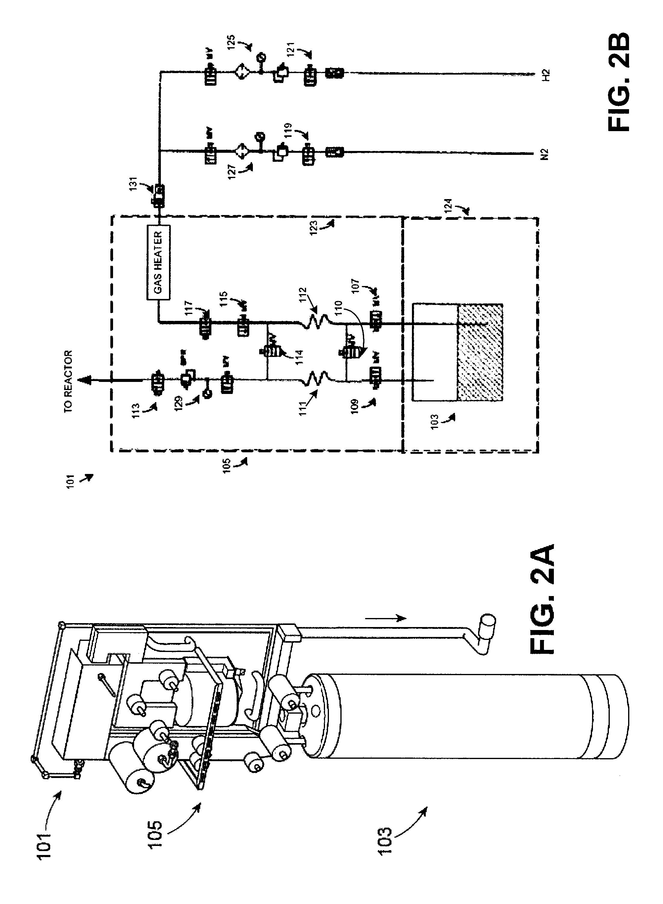
[0121]A conventional HVPE system consists of a hot-wall tube furnace usually fabricated of quartz. The Group III precursor is formed in-situ in the reactor by flowing HCl over a boat holding the Group III metal in a liquid form. The Group V precursor is supplied from external storage, e.g., a high pressure cylinder. Conventional HVPE has been used for the growth of arsenide, phosphide and nitride semiconductors. For the growth of GaN, the Group III source is typically molten Ga in a quartz boat (with which the HCl reacts to form GaCl), and the Group V source is usually ammonia gas.

[0122]In more detail, the quartz tube can be orien...


PUM

PropertyMeasurementUnit
Temperatureaaaaaaaaaa
Timeaaaaaaaaaa
Massaaaaaaaaaa

Abstract

The present invention is related to the field of semiconductor processing equipment and methods and provides, in particular, methods and equipment for the sustained, high-volume production of Group III-V compound semiconductor material suitable for fabrication of optic and electronic components, for use as substrates for epitaxial deposition, for wafers and so forth. In preferred embodiments, these methods are optimized for producing Group III-N (nitrogen) compound semiconductor wafers and specifically for producing GaN wafers. Specifically, the method includes reacting an amount of a gaseous Group III precursor as one reactant with an amount of a gaseous Group V component as another reactant in a reaction chamber under conditions sufficient to provide sustained high volume manufacture of the semiconductor material on one or more substrates, with the gaseous Group III precursor continuously provided at a mass flow of 50 g Group III element/hour for at least 48 hours. A system for conducting the method is also provided.

Description

FIELD OF THE INVENTION[0001]The present invention relates to the field of semiconductor processing equipment and methods, and provides, in particular, equipment and methods for the high volume manufacturing of Group III-V compound semiconductor wafers that are suitable for fabrication of optic and electronic components, for use as substrates for epitaxial deposition, and so forth. In preferred embodiments, the equipment and methods are directed to producing Group III-nitride semiconductor wafers, and specifically to producing gallium nitride (GaN) wafers.BACKGROUND OF THE INVENTION[0002]Group III-V compounds are important and widely used semiconductor materials. Group III nitrides in particular have wide, direct band gaps, which make them particularly useful for fabricating optic components (particularly, short wavelength LEDs and lasers) and certain electronic components (particularly, high-temperature / high-power transistors).[0003]The Group III nitrides have been known for decades...

Claims


Application Information

Patent Timeline
IPC IPC(8): C30B25/10C23C16/34B01F23/10
CPCC23C16/303C23C16/4411C23C16/4412C23C16/45504C23C16/45593C30B25/10C30B29/406C30B35/00H01L21/0254H01L21/0262C30B25/14H01L21/20H01L27/12H01L21/673C22B7/00
Inventor ARENA, CHANTALWERKHOVEN, CHRISTIAAN
Owner S O I TEC SILICON ON INSULATOR THECHNOLOGIES
Why Eureka
Try Eureka