Method for Producing Diamond Having Acicular Projection Array Structure on Surface thereof, Diamond Material, Electrode and Electronic Device

a diamond and acicular technology, applied in the field of methods, can solve the problems of electrode performance decline, high attempts to obtain diamonds, and the porosity of a porous body has so far a tendency to decline under mechanical pressure in molding, and achieves excellent electrode characteristics, high negative electron affinity and electron emission capabilities, and excellent electrode characteristics.

Inactive Publication Date: 2009-10-15
CENTRAL JAPAN RAILWAY COMPANY
View PDF1 Cites 28 Cited by
  • Summary
  • Abstract
  • Description
  • Claims
  • Application Information

AI Technical Summary

Benefits of technology

[0028]For example, by applying hydrogen plasma or performing hydrogen annealing treatment to the oxygen-terminated diamond surface, the diamond surface can be hydrogen-terminated. The hydrogen-terminated diamond has higher negative electron affinity and electron emission capabilities than an oxygen-terminated diamond. In other words, by experiencing a process of hydrogen-terminating the surface of acicular projections after a process of forming an acicular projection array structure by etching using oxygen plasma, a diamond with higher electron emission capabilities can be provided.
[0029]An electrode including a diamond material produced by the method for producing a diamond in the present invention has an excellent electrode characteristics with larger surface area due to an acicular projection array structure having high minuteness and aspect ratio. Therefore, this electrode is suitably applicable as a cathode for a lithium secondary battery, an electrode for a fuel cell, an electrode for ozone generation, an electrode for industrial electrolysis, an electrode for a chemical sensor, or an electrode for electron emission.
[0030]Also, an electronic device including, as a component, a diamond material produced by the method for producing a diamond in the present invention (an individual part which becomes a component of an equipment, an electronic circuit or the like with separate unique functions) has dramatically improved capabilities compared with the conventional devices, since the diamond material has a larger surface area and excellent electron emission capabilities. In particular, this diamond material is suitably applicable as a component of a lithium secondary battery, a fuel cell, an electric double layer capacitor, an electrolytic cell, a chemical sensor or an electron emission device.

Problems solved by technology

In addition, there is a tremendous amount of attempts recently to obtain a diamond with electrical conductivity by adding impurities.
Although such conventional electrodes are suitable in terms of conductivity and large surface area, since a porous carbon material has lower mechanical strength, a porosity of a porous body has so far a tendency to decline under a mechanical pressure in molding.
Since the declined porosity of a porous carbon material means smaller reaction area thereof, the electrode performance declines.

Method used


Image

  • Method for Producing Diamond Having Acicular Projection Array Structure on Surface thereof, Diamond Material, Electrode and Electronic Device
  • Method for Producing Diamond Having Acicular Projection Array Structure on Surface thereof, Diamond Material, Electrode and Electronic Device
  • Method for Producing Diamond Having Acicular Projection Array Structure on Surface thereof, Diamond Material, Electrode and Electronic Device

Examples


first embodiment

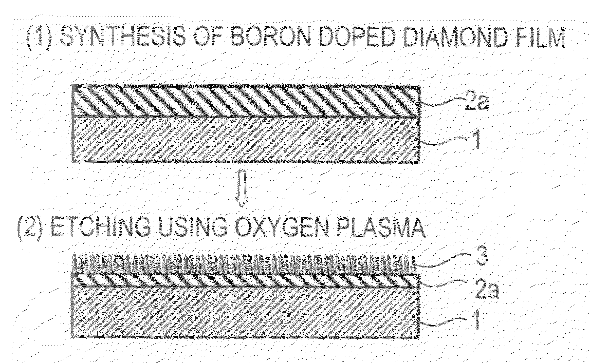
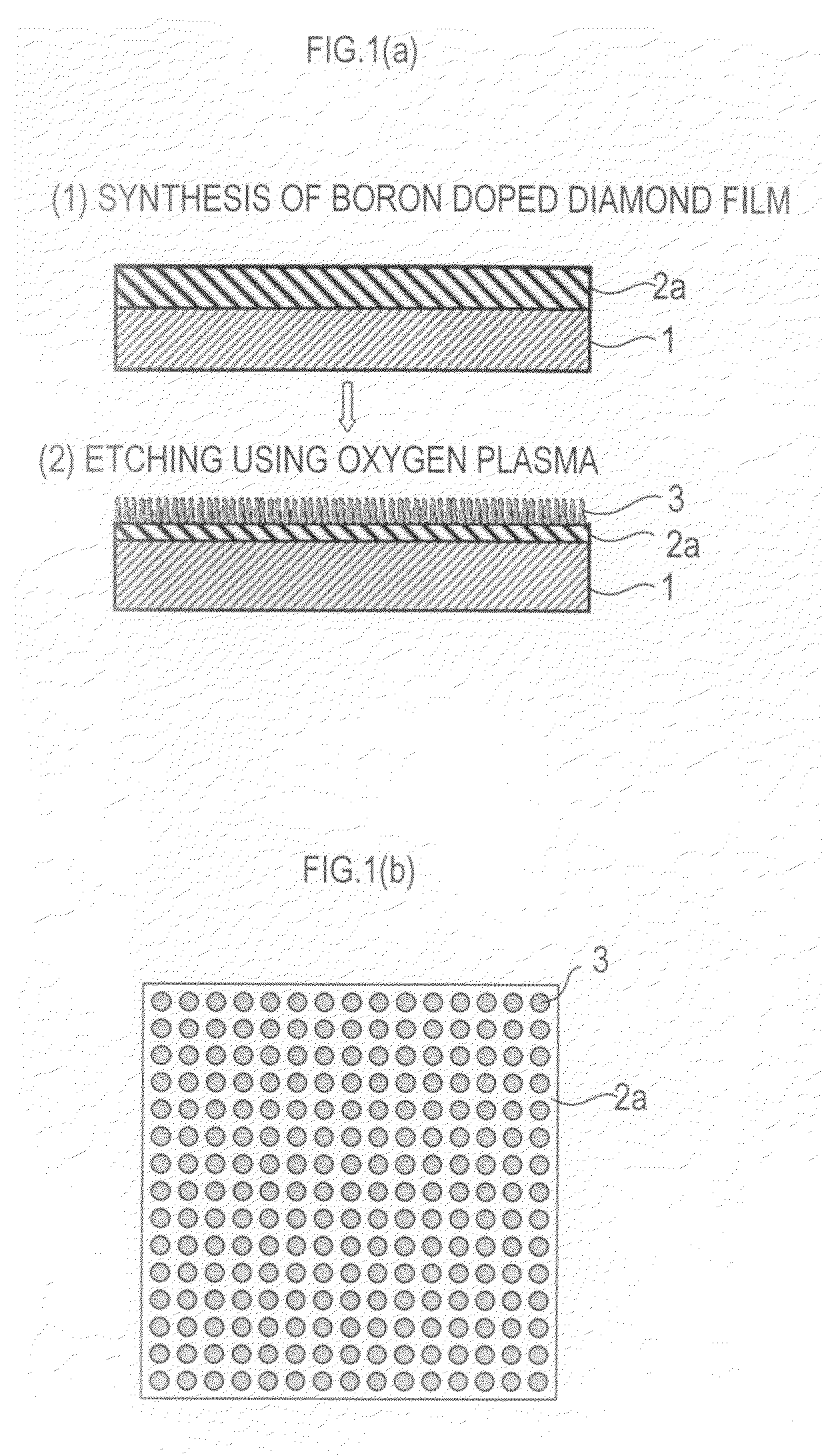
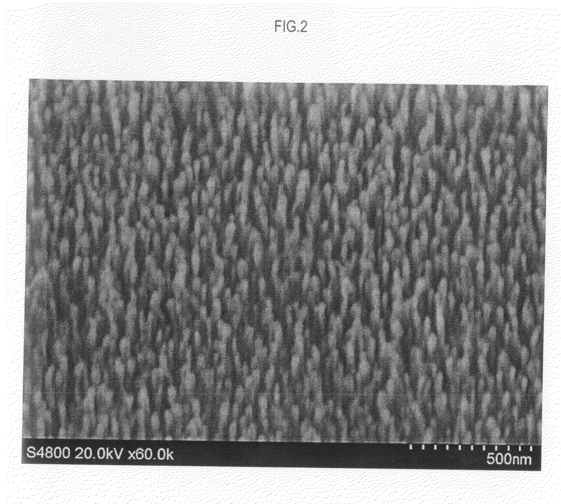
[0047]FIG. 1(a) is a schematic view showing a process of producing a diamond having an acicular projection array structure on the surface thereof (First Embodiment).

[0048]Firstly, as shown in (1) of FIG. 1(a), a boron-doped diamond film 2a, to which boron is incorporated, is generated on a substrate 1. An example of the methods for generating the boron-doped diamond film 2a includes a micro-wave plasma CVD method. Firstly, diamond seed crystals are applied on the substrate 1 (n-Si(111) substrate in the present embodiment) by mechanical polishing. Then, a gas is obtained by bubbling with hydrogen gas a solution (boron solution) in which boron oxide is dissolved in an acetone-methanol mixture solution. Using the obtained gas as sources of carbon and boron by the micro-wave plasma CVD method, the boron doped diamond film 2a is synthesized on the substrate 1.

[0049]In an experiment conducted by the inventors of the present invention, under conditions of a B / C ratio of 104 ppm in the abov...

second embodiment

[0056]FIG. 4 is a schematic diagram showing a process for producing a diamond device applicable as an electronic device such as an electron emission device and a chemical sensor (Second Embodiment).

[0057]Firstly, as shown in FIG. 4(1), a doped diamond film 2b is generated on a substrate 1. An appropriate dopant, such as boron, nitrogen and phosphorus is incorporated into diamond, and the doped diamond film 2b is produced in accordance with an intended use of a diamond material to be produced. Next, as shown in FIG. 4(2), a pattern of an insulating layer 4 is formed through general-purpose photolithography and etching treatment on the surface of the generated doped diamond film 2b. Also, the patterning may be performed after a gate electrode or the like is further overlayered on the insulating layer 4. Then, as shown in FIG. 4(3), a plurality of acicular projections 3 are formed on an exposed portion of the doped diamond film 2b in a pattern of the formed insulating layer 4 through r...

third embodiment

[0063]In the above-mentioned First and Second Embodiments, a dopant such as boron is added in a process of generating a diamond film. However, it may be also possible to incorporate a dopant to a specific site while controlling a dose amount by ion implantation or the like after a diamond synthesis, without adding a dopant in a process of generating a diamond through a chemical vapor deposition method or a high pressure high temperature synthetic method.

[0064]FIG. 5 is a schematic view showing a process of producing a diamond device in a case of forming acicular projections by adding a dopant through ion implantation after a diamond film synthesis (Third Embodiment).

[0065]Firstly, as shown in FIG. 5(1), a diamond film 2 (without doping) is synthesized on a substrate 1 by a micro-plasma CVD method. An example of the conditions for generating the film includes methane diluted with hydrogen into a concentration of 1% to be supplied as a carbon source gas, a substrate temperature of 850...


PUM

PropertyMeasurementUnit
pressureaaaaaaaaaa
depthaaaaaaaaaa
thicknessaaaaaaaaaa

Abstract

A method for producing a diamond having an acicular projection array structure on a surface thereof comprises the step of forming the acicular projection array structure on a surface of a diamond base material by treating the surface of the diamond base material by dry etching using oxygen gas. At least one dopant selected among boron (B), nitrogen (N), aluminum (Al), silicon (Si), phosphorus (P), sulfur (S), copper (Cu), arsenic (As), molybdenum (Mo), platinum (Pt) and gold (Au) is doped with a concentration of 1×10¹⁹ atoms/cm3 and more at least in a region near the surface of the diamond base material.

Description

TECHNICAL FIELD[0001]The present invention relates to a method for producing a diamond having a highly minute acicular projection array structure, which is suitable as a wide range of electrode materials or the like, on the surface thereof.BACKGROUND ART[0002]It is expected that a carbon material is applied to a cathode for a lithium secondary battery, an electrode for a fuel cell, an electrode for electron emission, an electrode for industrial electrolysis, an electrode for a chemical sensor, an electrode for an electronic device, an electron emission device or the like. Large surface area of carbon material with acicular projection array structure is suitable for the above-mentioned applications.[0003]Carbon has both ordered structure and unordered structure, mainly composed of SP2 and SP3 bonded. Four allotropes which are derived from such structure, noncrystalline carbon (amorphous), graphite, fullerene and diamond, are known. Among carbon materials including these allotropes, a...

Claims


Application Information

Patent Timeline
Patent Type & Authority Applications(United States)
IPC IPC(8): H01M4/02H01M4/04H01M4/96C25B11/12H01M4/58C23C16/27C23C16/56C30B29/04C30B33/12H01M4/583
CPCC30B29/04C30B33/12H01M4/133H01M4/583Y10T428/24355H01M4/96Y02E60/122Y02E60/50H01M4/625Y02E60/10H01M4/02
Inventor TERASHIMA, CHIAKIARIHARA, KAZUKIFUJISHIMA, AKIRA
Owner CENTRAL JAPAN RAILWAY COMPANY
Why Eureka
Try Eureka