Method of manufacturing dielectric film

a manufacturing method and dielectric film technology, applied in the field of manufacturing dielectric film and semiconductor devices, can solve the problems of sputtering method, slowing down the deposition rate of dielectric films, and reducing the sputtering rate, so as to achieve superior flatness and higher permittivity

Active Publication Date: 2010-09-02
CANON ANELVA CORP
View PDF22 Cites 7 Cited by
  • Summary
  • Abstract
  • Description
  • Claims
  • Application Information

AI Technical Summary

Benefits of technology

[0033]According to the present invention, a dielectric film having (1) a relative permittivity value of 40 or higher, (2) heat resistance with respect to high-temperature annealing at 1000° C., and (3) superior flatness can be obtained. Consequently, even when the method of manufacturing a dielectric film according to the present invention is applied to method of manufacturing a gate insulating film of a CMOS transi

Problems solved by technology

However, the techniques described above respectively have the following problems.
With the technique described in Patent Document 1 in which Al is included within a range of 5 to 30% in ZrO2, a problem arises in that while a high relative permittivity value of 25 to 28 is obtained with a noncrystalline structure, the value is nevertheless lower than the relative permittivity value of 30 of ZrO2 having a crystalline structure.
The technique described in Patent Document 2 of forming ZrO2 utilizing electron cyclotron resonance is problemat

Method used


Image

  • Method of manufacturing dielectric film
  • Method of manufacturing dielectric film
  • Method of manufacturing dielectric film

Examples


first example

Example Using Cosputtering

[0100]A first example of the present invention will now be described in detail with reference to the drawings.

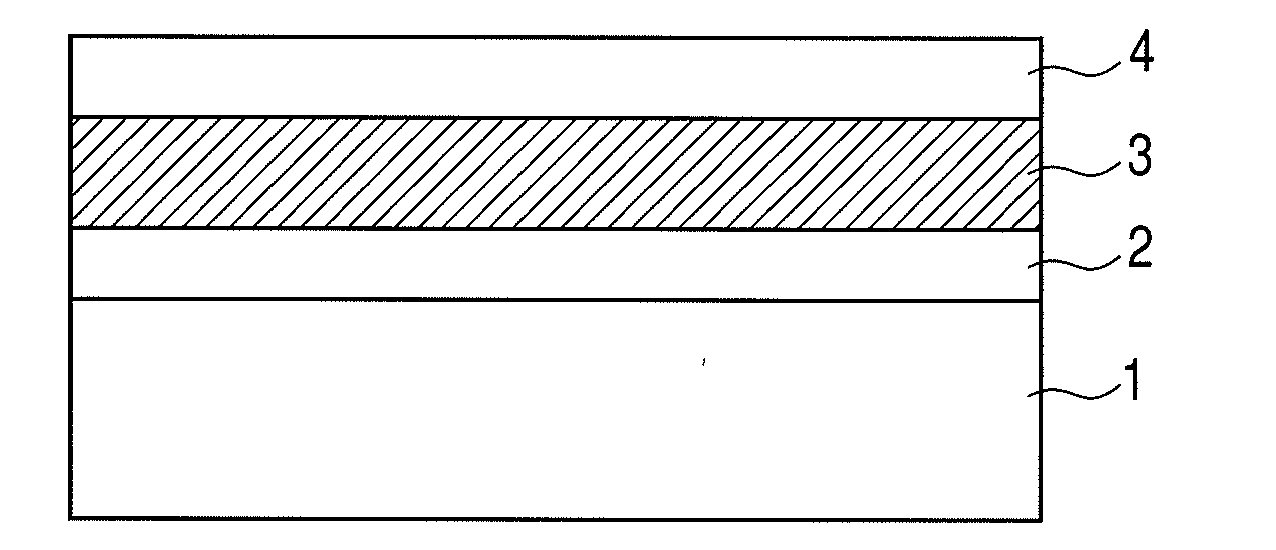
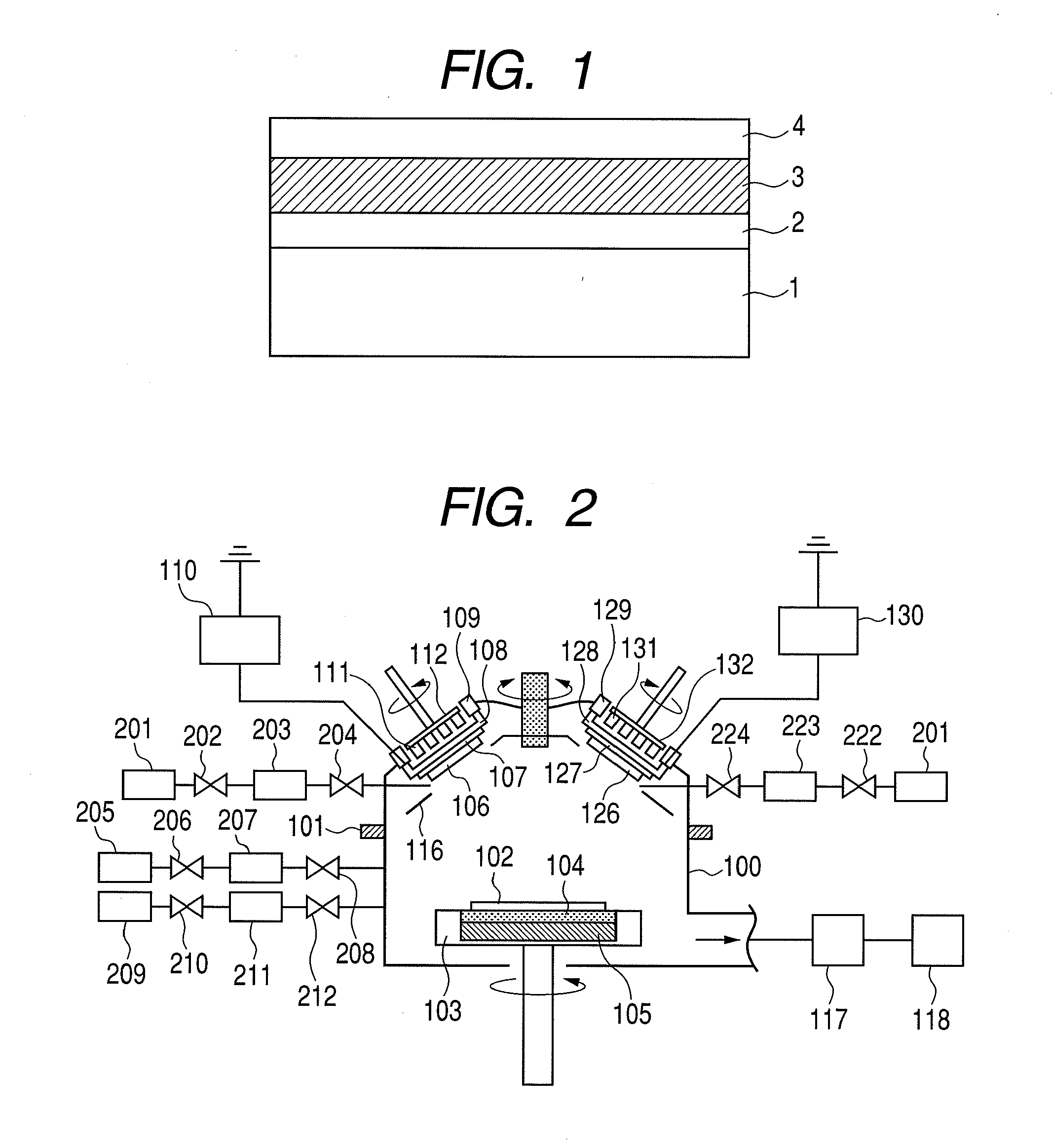
[0101]FIG. 18 is a diagram illustrating an MIS capacitor having a dielectric film formed by the method according to the present invention. A substrate processing apparatus according to the present example such as that illustrated in FIG. 2 deposited a HfAlON film 303 having a noncrystalline structure by a sputtering method on a silicon substrate 301 having, on a surface thereof, a silicon dioxide film 302 with a film thickness ranging from 3 nm to 5 nm. Metallic targets of Hf and Al were used as the targets 106 and 126. Argon, oxygen, and nitrogen were used as sputtering gases.

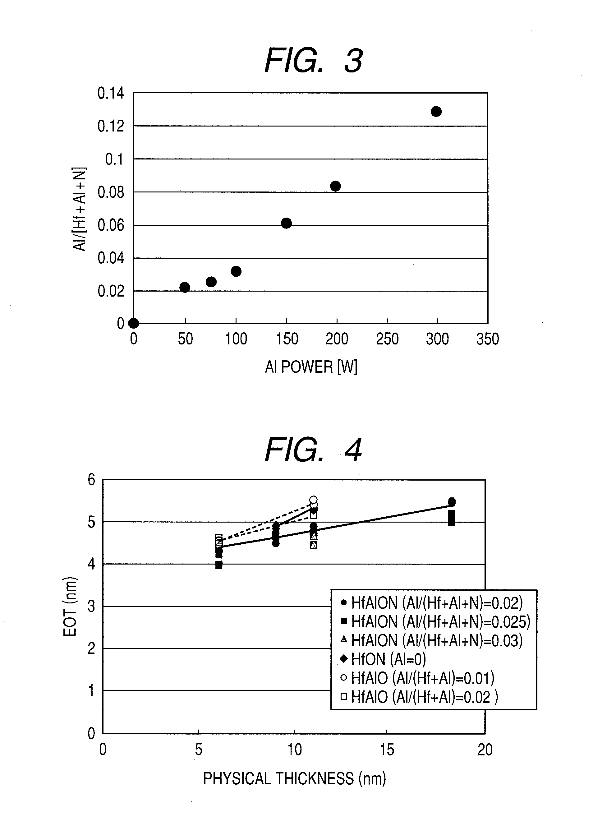
[0102]A substrate temperature can be arbitrarily set within a range of 27° C. to 600° C., a target power to within a range of 50 W to 1000 W, a sputter gas pressure to within a range of 0.02 Pa to 0.1 Pa, an Ar gas flow rate to within a range of 1 sccm to 200 sccm, an oxygen g...

second example

Example Applied to Gate Insulating Film

[0116]A second example of the present invention will now be described in detail with reference to the drawings.

[0117]FIG. 19 is a diagram illustrating processes of a semiconductor device manufacturing method according to a second example of the present invention.

[0118]First, as depicted by process 1 in FIG. 19, a substrate processing apparatus according to the present example forms an element isolation region 402 on a surface of a silicon substrate 401 using a STI (shallow trench isolation) technique. The substrate processing apparatus according to the present example then forms a silicon dioxide film 403 with a film thickness of 1.8 nm on the element-isolated surface of the silicon substrate 401 using a thermal oxidation method. Subsequently, the substrate processing apparatus according to the present example forms a HfAlON film with a film thickness ranging from 1 nm to 10 nm using the same method as the first example. Next, the substrate pro...

third example

Example Applied to Blocking Film of Non-Volatile Memory Element

[0123]FIG. 20 is a cross-sectional diagram illustrating fabricating processes of a semiconductor element according to a third example of the present invention.

[0124]First, as depicted by process 1 in FIG. 20, a substrate processing apparatus according to the present example forms an element isolation region 502 on a surface of a silicon substrate 501 using a STI (shallow trench isolation) technique. The substrate processing apparatus according to the present example then forms a silicon dioxide film as a first insulating film 503 to 30 Å to 100 Å on the element-isolated surface of the silicon substrate 501 using a thermal oxidation method. Subsequently, the substrate processing apparatus according to the present example forms a silicon nitride film as a second insulating film 504 to 30 Å to 100 Å using an LPCVD (low pressure chemical vapor deposition) method. Next, the substrate processing apparatus according to the pres...


PUM

PropertyMeasurementUnit
Temperatureaaaaaaaaaa
Fractionaaaaaaaaaa
Forceaaaaaaaaaa

Abstract

The present invention provides a method of manufacturing a dielectric film having a high permittivity. An embodiment of the present invention is a method of manufacturing, on a substrate, a dielectric film including a metallic oxynitride containing an element A made of Hf or a mixture of Hf and Zr, an element B made of Al, and N and O. The manufacturing method includes: a step of forming a metallic oxynitride whose mole fractions of the element A, the element B, and N expressed as B/(A+B+N) has a range of 0.015≦(B/A+B+N))≦0.095 and N/(A+B+N) has a range of 0.045≦(N/(A+B+N)) and a mole fraction O/A of the element A and O has a range expressed as 1.0<(O/A)<2.0, and having a noncrystalline structure; and a step of performing an annealing treatment at 700° C. or higher on the metallic oxynitride having a noncrystalline structure to form a metallic oxynitride including a crystalline phase with a cubical crystal incorporation percentage of 80% or higher.

Description

CROSS-REFERENCES TO RELATED APPLICATIONS[0001]This application is a continuation application of International Application No. PCT / JP2009 / 065306, filed on Sep. 2, 2009, the entire contents of which are incorporated by reference herein.[0002]This application also claims the benefit of priority from Japanese Patent Application No. 2008-282163 filed Oct. 31, 2008, the entire contents of which are incorporated herein by reference.TECHNICAL FIELD[0003]The present invention relates to a method of manufacturing a dielectric film and a semiconductor device using a dielectric film.BACKGROUND ART[0004]Developments in semiconductor devices are accompanied by increasingly higher degrees of element integration, resulting in increased miniaturization of each element and a reduction in operating voltage. For example, in the field of MONOS (metal oxide nitride oxide semiconductor)-type non-volatile semiconductor devices which include a blocking film that separates a charge retaining layer and a gate...

Claims


Application Information

Patent Timeline
IPC IPC(8): H01L21/336H01L21/28G06F19/00C23C14/35C01B21/20C23C14/06C23C14/58H01L21/316H01L21/318H01L21/822H01L21/8247H01L27/04H01L27/115H01L29/78H01L29/788H01L29/792
CPCC23C14/0676H01L29/7881C23C14/3464H01L21/02178H01L21/02181H01L21/02194H01L21/02266H01L21/28273H01L21/28282H01L21/31604H01L21/318H01L29/42324H01L29/4234H01L29/513C23C14/225H01L29/40114H01L29/40117
Inventor KITANO, NAOMUNAKAGAWA, TAKASHITATSUMI, TORU
Owner CANON ANELVA CORP
Why Eureka
Try Eureka