

Method of forming semiconductor film and photovoltaic device including the film
a technology of photovoltaic devices and semiconductor films, applied in the direction of pv power plants, metal/alloy conductors, conductors, etc., can solve the problems of reducing using high-cost vacuum-based methods, and no reports of hydrazine-based deposition approaches for depositing homogeneous chalcogenide layers, etc., to avoid or reduce the need for enhancing additives, convenient elimination, and convenient us
- Summary
- Abstract
- Description
- Claims
- Application Information
AI Technical Summary
Benefits of technology
Problems solved by technology
Method used
Image

Examples
example 1
Preparation of Cu2ZnSn(S,Se)4Film
[0056]All operations were performed in nitrogen-filled glove box. The deposition solution was prepared in two parts in glass vials under magnetic stirring: A1, by dissolving Cu2S, 0.573 g and sulfur, 0.232 g in 3 ml of hydrazine and B1, by mixing SnSe, 0.790 g, Se, 1.736 g and Zn, 0.32 g with 7 ml of hydrazine. After 3 days under magnetic stirring, solution A had an orange transparent aspect, while B1 was dark green and opaque. Solutions A1 and B1 were mixed (C1) before deposition.
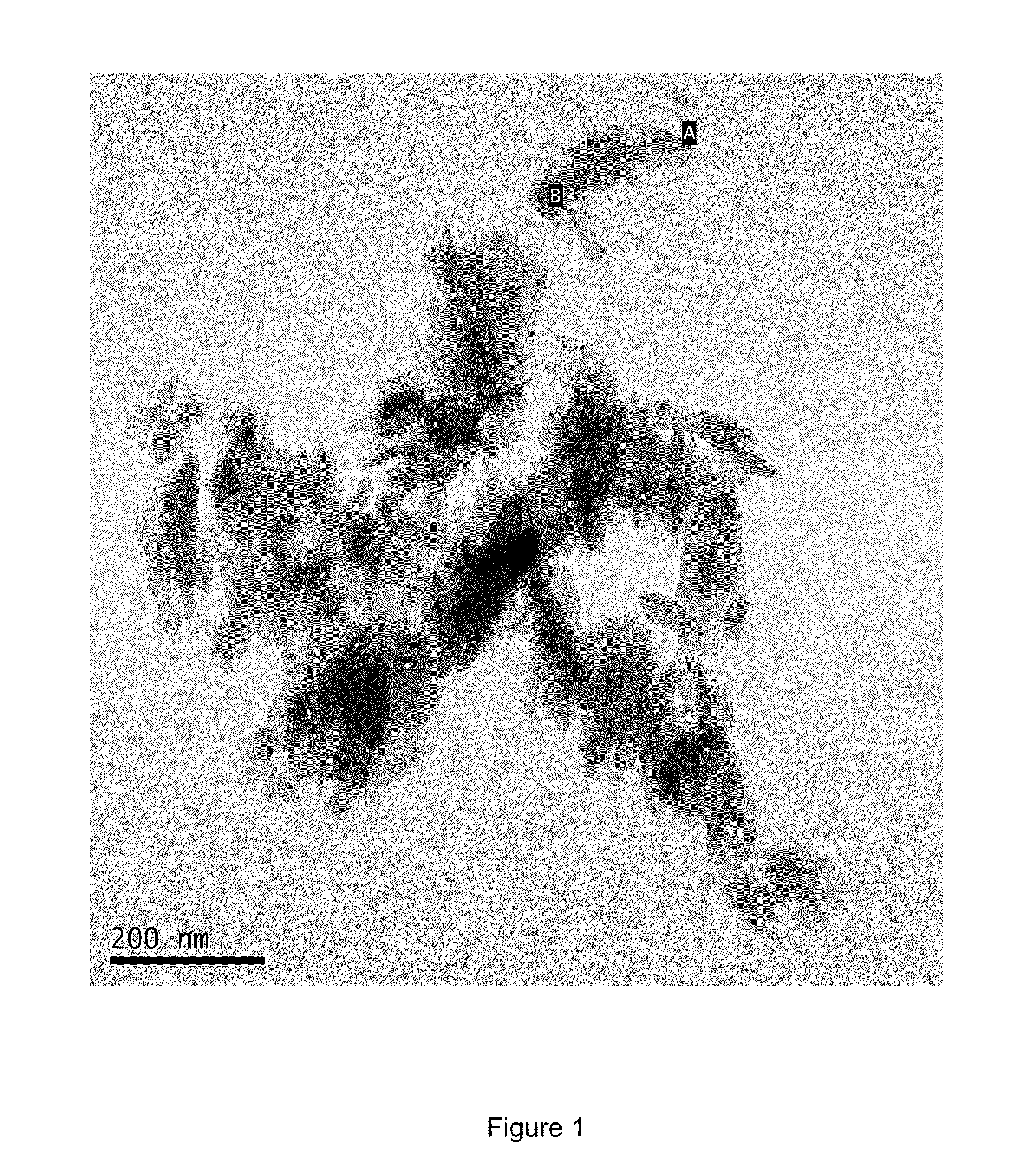
[0057]A sample of the mixed solution was filtered through a syringe filter and the filtered particles were observed by Transmission Electron Microscopy (FIG. 1). Particles are elongated with dimensions that can be represented by the formula d≧2 e wherein d is at least one dimension of the particles and e is any other dimension of the particles. For example, where d can be the length and e can be the width. EDX analysis confirmed presence of Zn and Se in the solid particles ...
example 2
Preparation of Cu2ZnSn(S,Se)4 Film
[0059]Repeating the procedure of Example 1, atmosphere containing elemental sulfur vapor (0.12 g / l N2) was used for the final anneal.
example 3
Photovoltaic Devices Prepared by the Method of the Present Invention
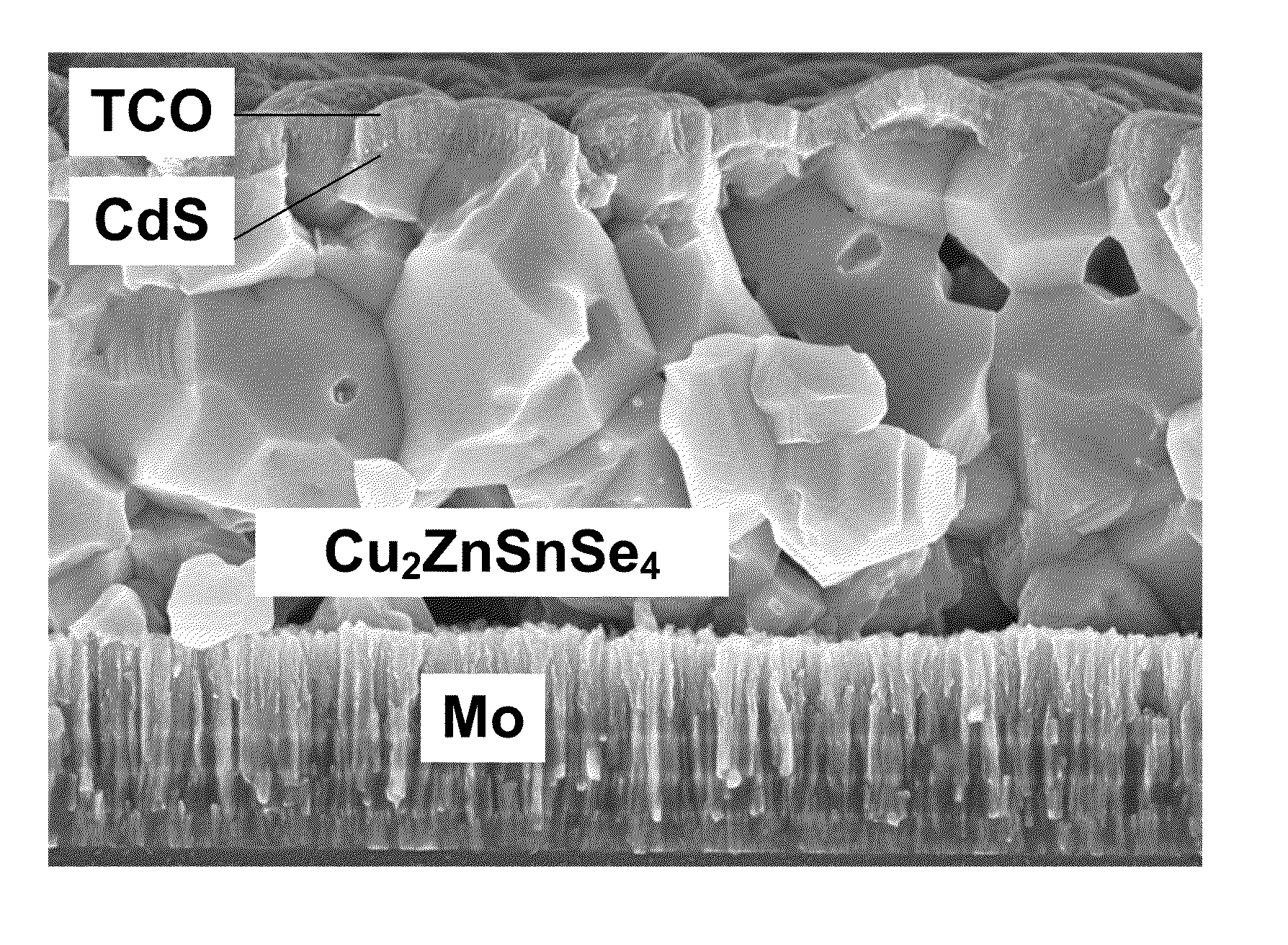
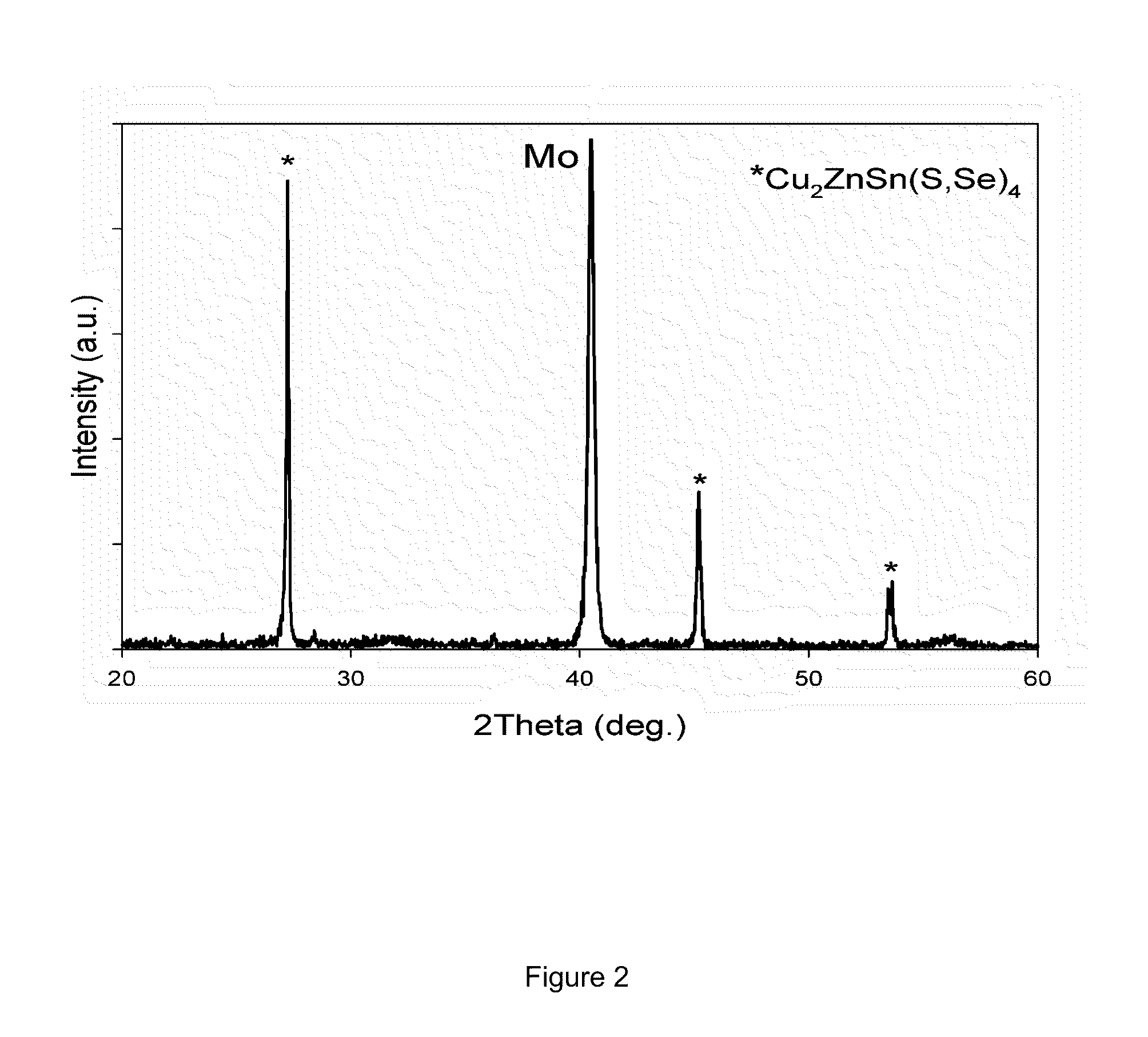
[0060]Solar cells were fabricated from the above-described Cu2ZnSn(Se,S)4 films by deposition of 60 nm CdS buffer layer by chemical bath deposition, 100 nm insulating ZnO and 130 nm ITO (indium-doped zinc oxide) by sputtering (FIG. 2). In addition to the shown structure, Ni / Al metal contacts and 110 nm MgF coatings were deposited by electron-beam evaporation.
[0061]Photovoltaic performance was measured (NREL CERTIFIED, FIG. 4) under ASTM G173 global spectrum, yielding 9.3% efficiency with films prepared according to Example 1 and 9.66% total area, including metal contacts, i.e., about 5% of the total area, conversion efficiency with films prepared according to example 2, with Voc=0.5160 V, Isc=12.481 mA, Jsc=28.612 mA / cm2, Fill Factor=65.43% (FIG. 4).
[0062]The potential advantage of this process is that it would be much lower cost than the traditional approaches. This performance is a world record for the category of...
PUM
 Abstract
Description
Claims
Application Information