Sintered complex oxide and sputtering target comprising same

Inactive Publication Date: 2011-10-06
IDEMITSU KOSAN CO LTD
View PDF3 Cites 22 Cited by
  • Summary
  • Abstract
  • Description
  • Claims
  • Application Information

AI Technical Summary

Benefits of technology

[0021]The invention thus provides a composite oxide sintered body that makes it possible to produce a TFT panel with improved

Problems solved by technology

However, since a high temperature (e.g., 800° C. or more) is required to crystallize a crystalline silicon thin film, it is difficult to form a crystalline silicon thin film on a glass substrate or an organic substrate.
Therefore, a crystalline silicon thin film can only be formed on an expensive heat-resistant substrate (e.g., silicon wafer or quartz).
Moreover, a large amount of energy and a large number of steps are required to produce a crystalline silicon thin film.
Since the device structure of a thin film transistor (TFT) that utilizes a crystalline silicon thin film is normally limited to a top-gate structure, it is difficult to reduce cost by reducing the number of masks, for example.
Therefore, when using an amorphous silicon semiconductor thin film for a switching device for driving a display, a high-speed animation may not be displayed.
However, it is difficult to industrially apply a transparent semiconductor thin film formed of a metal oxide (particularly a transparent semiconductor thin film formed by crystallizing zinc oxide at a high temperature) due to low field-effect mobility (hereinafter may be referred to as “mobility”) (about 1 cm2/V·sec), a small on-off ratio, and occurrence of leakage current.
A crystalline oxide semiconductor that contains zinc oxide has been extensively studied, but has the following problems when film formation is conducted by sputtering.
For example, an oxide semiconductor film formed of a conductive transparent oxide that contains zinc oxide as the main component tends to produce a large number of carrier electrons due to oxygen defects, so that it is difficult to reduce conductivi

Method used


Image

  • Sintered complex oxide and sputtering target comprising same
  • Sintered complex oxide and sputtering target comprising same

Examples


example 1

Production of Composite Oxide Sintered Body

[0190]The following oxide powders were used as starting raw material powders. The specific surface area of each oxide powder was measured by the BET method.

(a) Indium oxide powder (specific surface area: 8 m2 / g)

(b) Gallium oxide powder (specific surface area: 8 m2 / g)

(c) Zinc oxide powder (Specific surface area: 5 m2 / g)

[0191]The oxide powders were weighed and mixed so that the ratio “(a):(b):(c)” was 50:35:15 (wt %) to prepare a raw material powder mixture. The raw material powder mixture had a specific surface area of 6.3 m2 / g.

[0192]The raw material powder mixture was mixed and ground using an agitator bead mill with a wet medium while checking the specific surface area of the powder mixture. The specific surface area of the ground powder mixture was larger than that of the raw material powder mixture by 2 m2 / g.

[0193]Zirconia beads having a diameter of 1 mm were used as the media of the agitator bead mill with a wet medium.

[0194]The ground ...

examples 2 to 7

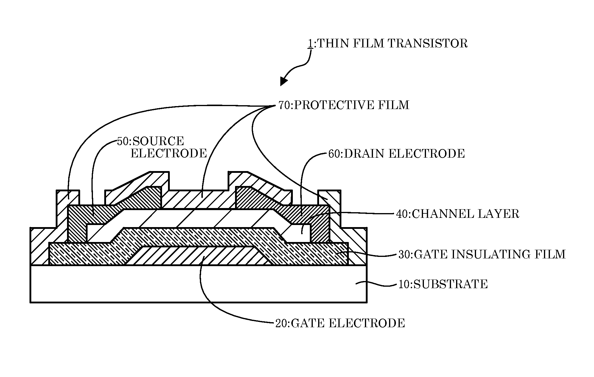
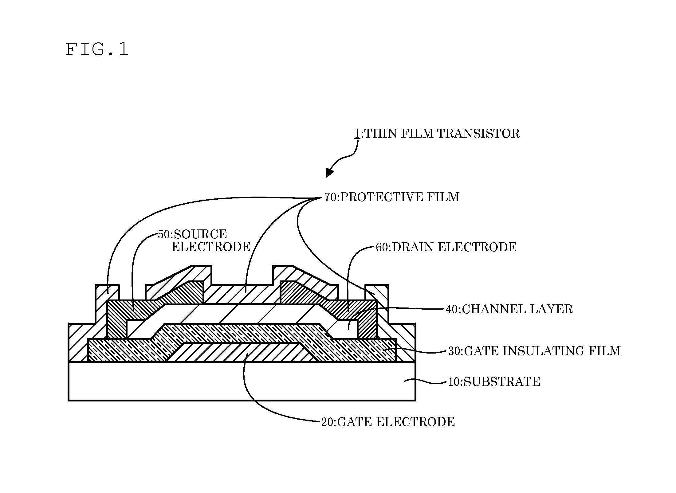
[0218]A sintered body was produced and evaluated, and a TFT panel was produced and evaluated in the same manner as in Example 1, except for using starting raw material powders shown in Table 1, and producing the sintered body under conditions shown in Table 1. The results are shown in Table 1.

examples 8 to 15

[0219]A sintered body was produced and evaluated, and a TFT panel was produced and evaluated in the same manner as in Example 1, except for using starting raw material powders shown in Table 2, and producing the sintered body under conditions shown in Table 2. The results are shown in Table 2.

[0220]In Examples 8 to 15, tin oxide, zirconium oxide, germanium dioxide, cerium oxide, niobium oxide, tantalum oxide, molybdenum oxide, or tungsten oxide (i.e., oxide of a metal element having a positive valence of 4 or more) was used as the starting raw material powder so that the atomic ratio of the metal element having a positive valence of 4 or more to the total metal elements was 0.0005.

[0221]As shown in Table 2, the evaluation results for the relative density, a variation in relative density, the bulk resistance, and the average hole count were improved.


PUM

PropertyMeasurementUnit
Temperatureaaaaaaaaaa
Lengthaaaaaaaaaa

Abstract

A composite oxide sintered body includes In2Ga2ZnO7 having a homologous crystal structure, and has a relative density of 90% or more, and an average crystal grain size of 10 μm or less.

Description

TECHNICAL FIELD[0001]The invention relates to a composite oxide sintered body that includes In2Ga2ZnO7 having a homologous crystal structure, a sputtering target that includes the composite oxide sintered body, an amorphous oxide film obtained using the sputtering target, and a thin film transistor that includes the amorphous oxide film.BACKGROUND ART[0002]A field effect transistor has been widely used as a unit electronic device of a semiconductor memory integrated circuit, a high-frequency signal amplifier device, a liquid crystal drive device, and the like. The field effect transistor is an electronic device that is most widely put to practical use at present.[0003]In recent years, development of displays has rapidly progressed, and a thin film transistor (TFT) has been widely used for a display (e.g., liquid crystal display (LCD), electroluminescence (EL) display, or field emission display (FED)) as a switching device for applying a driving voltage to the display element.[0004]A...

Claims


Application Information

Patent Timeline
IPC IPC(8): H01B1/02C01G9/02C23C14/08C04B35/64
CPCC04B35/453H01L29/7869C04B35/62655C04B35/62695C04B2235/3229C04B2235/3244C04B2235/3251C04B2235/3256C04B2235/3258C04B2235/3284C04B2235/3286C04B2235/3287C04B2235/3293C04B2235/5409C04B2235/604C04B2235/656C04B2235/6562C04B2235/6567C04B2235/658C04B2235/6585C04B2235/661C04B2235/664C04B2235/721C04B2235/722C04B2235/763C04B2235/77C04B2235/775C04B2235/786C04B2235/80C04B2235/81C04B2235/9661C23C14/086C23C14/3414C04B35/6261C04B35/64C23C14/34H01L21/02658H01L29/2206H01L29/242
Inventor YANO, KOKIKAWASHIMA, HIROKAZU
Owner IDEMITSU KOSAN CO LTD
Why Eureka
Try Eureka