Material structure for low thermal resistance silicon-based gallium nitride microwave and millimeter-wave devices and manufacturing method thereof

Pending Publication Date: 2022-09-29
XIDIAN UNIV
View PDF0 Cites 0 Cited by
  • Summary
  • Abstract
  • Description
  • Claims
  • Application Information

AI Technical Summary

Problems solved by technology

However, limited by relatively high price and relatively small size of silicon carbide substrate, the cost of SiC-based GaN device is relatively high.
However, compared with the SiC-based GaN device, a main disadvantage of the silicon-based GaN device is that its thermal resistance is relatively high, resulting in poor heat dissipation performance, which limits the output power of silicon-based GaN microwave and millimeter-wave devices.
Firstly, the thermal conductivity of the silicon substrate is relatively poor, and typically the thermal conductivity of the SiC substrate is 4.0 W/cm·K, while the thermal conductivity of the silicon substrate is only 1.5 W/cm·K.
Secondly, when a GaN based material is epitaxially grown on the silicon substrate, because a lattice mismatch between silicon and the GaN crystal material is relatively large, it is necessary to insert very thick nucleation layer and transition layer, such as an AlGaN material with graded aluminum composition or an aluminum nitride/gallium nitride superlattice material, between the active structure of GaN device and the silicon substrate.
The crystalline material of the nucleation layer and transition layer has relatively poor quality, excessive defects and poor thermal conductivity.
Heat generated by the device itself cannot be dissipated in time by the buffer layer, the nucleation layer, the transition layer and the substrate, which causes heat to accumulate in the channel as a significant self-heating effect.
Moreover, a lattice mismatch and defects of the boundary would increase the TBR.
1. after a device bare core process is completed, thinning the silicon substrate as much as possible, and then transferring the device with the thinned substrate to a heat sink with high thermal conductivity after dicing. At present, most of products of silicon-based GaN microwave and millimeter wave devices are to thin the silicon substrate to 100 μm, and a technology under development is to thin the silicon substrate to 50 μm. For example, A. Pantellini, A. Nanni, and C. Lanzieri have published a paper entitled “Thermal behavior of AlGaN/GaN HEMT on silicon Microstrip technology” on 6th European Microwave Integrated Circuit Conference on October 2011, in which a method is proposed to improve a heat dissipation performance of device by thinning a silicon substrate. However, a disadvantage of this method is that the process operation difficulty after thinning the silicon substrate is large, resulting in a decrease in the yield of device.
2. depositing layers of high thermal conductivit...

Method used


Image

  • Material structure for low thermal resistance silicon-based gallium nitride microwave and millimeter-wave devices and manufacturing method thereof
  • Material structure for low thermal resistance silicon-based gallium nitride microwave and millimeter-wave devices and manufacturing method thereof
  • Material structure for low thermal resistance silicon-based gallium nitride microwave and millimeter-wave devices and manufacturing method thereof

Examples


embodiment 1

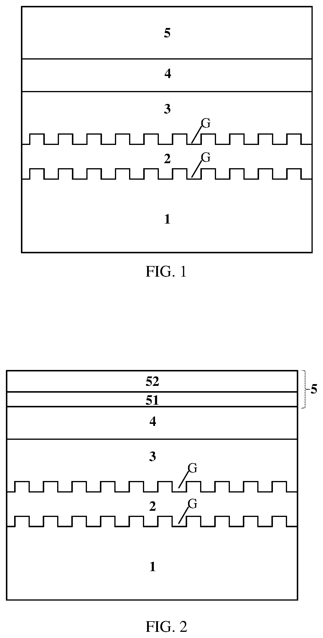
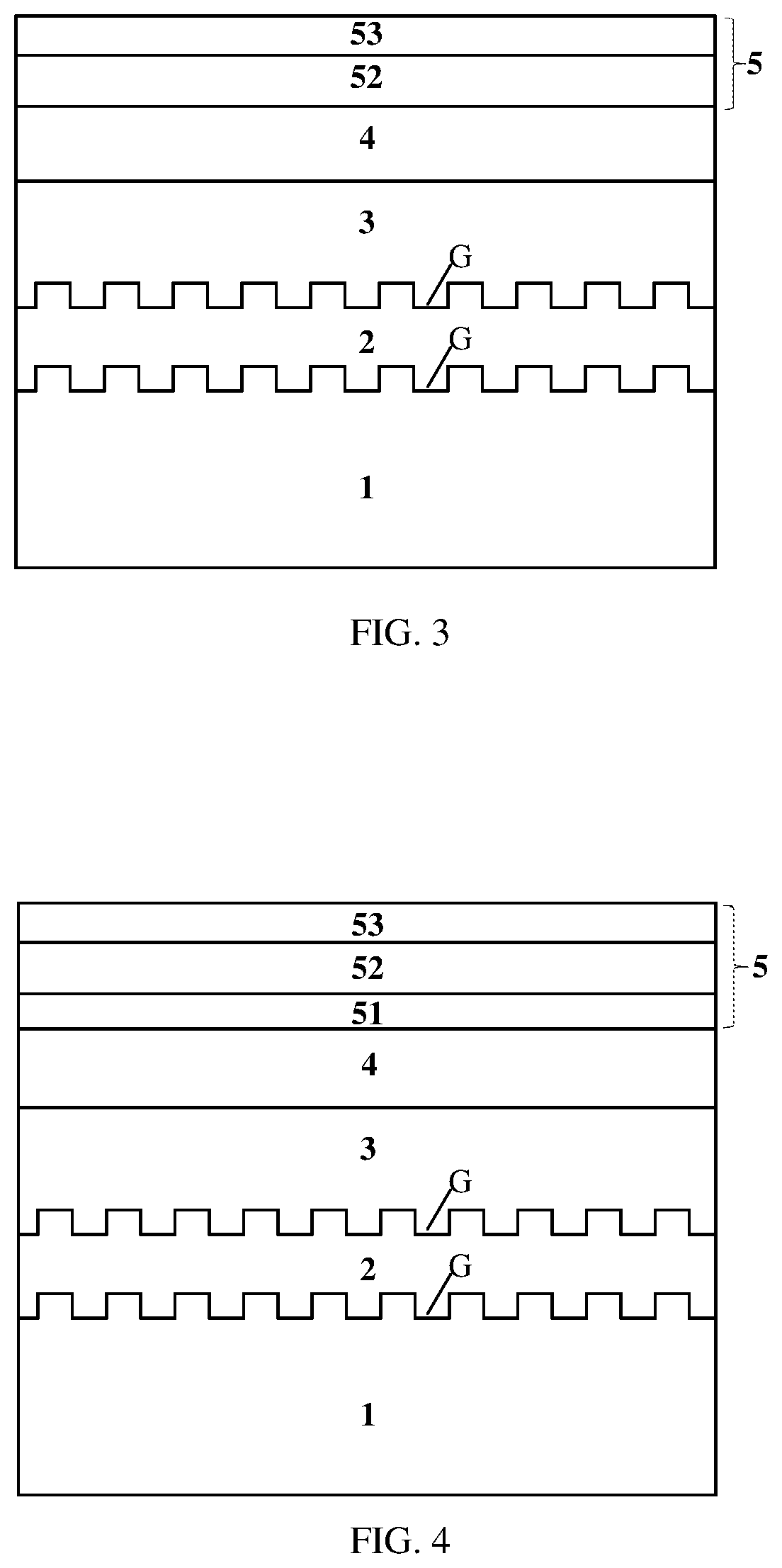
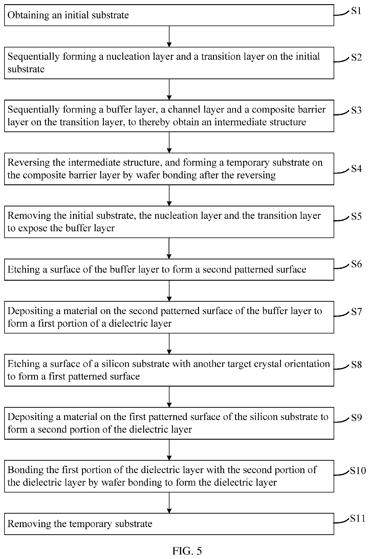
[0044]Referring to FIG. 1, and FIG. 1 is a schematic structural view of a material structure for low thermal resistance silicon-based GaN microwave and millimeter-wave devices according to the disclosure. The material structure for low thermal resistance silicon-based GaN microwave and millimeter-wave devices includes: a silicon substrate 1, a dielectric layer 2 of high thermal conductivity, a buffer layer 3, a channel layer 4 and a composite barrier layer 5.

[0045]The dielectric layer 2 is disposed on (for example, in contact with) the upper surface of the silicon substrate 1, and an uneven first patterned interface is formed between the dielectric layer 2 and the silicon substrate 1. The buffer layer 3 is disposed on (for example, in contact with) the upper surface of the dielectric layer 2, and an uneven second patterned interface is formed between the buffer layer 3 and the dielectric layer 2. The channel layer 4 is disposed on (for example, in contact with) the upper surface of ...

embodiment 2

[0068]On the basis of the above embodiment 1, this embodiment provides a manufacturing method of a material structure for low thermal resistance silicon-based GaN microwave and millimeter-wave devices.

[0069]Referring to FIG. 5 and FIGS. 6a-6t, and FIG. 5 is a schematic flowchart of the manufacturing method of a material structure for low thermal resistance silicon-based GaN microwave and millimeter-wave devices, and FIGS. 6a-6t are schematic structural views associated with a process of the manufacturing method of a material structure for low thermal resistance silicon-based GaN microwave and millimeter-wave devices. The manufacturing method may include steps as follows.

[0070]S1, obtaining an initial substrate 11. A material of the initial substrate 11 may be a silicon base with a target crystal orientation, as shown in FIG. 6a.

[0071]The illustrated embodiment uses the silicon base with the target crystal orientation as the initial substrate 11, and the silicon base is a high resis...


PUM


Abstract

A material structure for silicon-based gallium nitride microwave and millimeter-wave devices and a manufacturing method thereof are provided. The material structure includes: a silicon substrate; a dielectric layer of high thermal conductivity, disposed on an upper surface of the silicon substrate, and an uneven first patterned interface being formed between the dielectric layer and the silicon substrate; a buffer layer, disposed on an upper surface of the dielectric layer, and an uneven second patterned interface being formed between the buffer layer and the dielectric layer; a channel layer, disposed on an upper surface of the buffer layer; and a composite barrier layer, disposed on an upper surface of the channel layer. In the material structure, the uneven patterned interfaces increase contact areas of the interfaces, a thermal boundary resistance and a thermal resistance of device are reduced, and a heat dissipation performance of device is improved.

Description

FIELD OF THE DISCLOSURE[0001]The disclosure relates to the field of semiconductor devices, and more particularly to a material structure for low thermal resistance silicon-based gallium nitride microwave and millimeter-wave devices and a manufacturing / preparing method thereof.BACKGROUND OF THE DISCLOSURE[0002]With the development of microelectronics technologies, a third-generation wide bandgap semiconductor material represented by gallium nitride (GaN) has a large band gap, a high critical breakdown electric field, a high electron saturation drift velocity, a stable chemical performance, and physical properties such as high temperature resistance and radiation resistance. The use of a GaN material for preparing an electronic device can further reduce a chip area, increase an operating / working frequency, increase an operating temperature, reduce an on-resistance and increase a breakdown voltage. The GaN material has great potential in the preparation of microwave and millimeter-wave...

Claims


Application Information

Patent Timeline
IPC IPC(8): H01L29/20H01L29/06H01L23/373
CPCH01L29/2003H01L29/0684H01L23/3738H01L29/778H01L23/373H01L29/7786H01L29/0649H01L21/0254H01L21/02458H01L21/02488H01L21/02505H01L21/02494H01L21/0243H01L21/02433H01L21/02381H01L21/7624H01L29/872
Inventor ZHANG, JINCHENGHAO, LULIU, ZHIHONGLIU, JUNWEISONG, KUNLUZHANG, YACHAOZHANG, WEIHANGHAO, YUE
Owner XIDIAN UNIV
Why Eureka
Try Eureka