Coating, modification and etching of substrate surface with particle beam irradiation of the same

a technology of etching and substrate surface, applied in the field of surface treatment technology, can solve the problems of copper-based conductors, voids or seams in copper filled recesses, and the interlayer insulative film layer of silicon oxide and an aluminum-based conductor is confronted with serious problems, and achieves favorable adhesion (bond) strength, high adhesion (bond) strength, and high bond strength.

Inactive Publication Date: 2005-07-26
EBARA CORP
View PDF10 Cites 79 Cited by
  • Summary
  • Abstract
  • Description
  • Claims
  • Application Information

AI Technical Summary

Benefits of technology

[0038]When mixing action occurs at a moderate depth, a bond strength between a substrate and a deposited film on a substrate surface becomes remarkably high. This phenomenon is considered to be due to the fact that atoms or molecules constituting the deposited film and the substrate are mixed together by the mixing action. In the process shown in FIG. 1, two materials that can hardly adhere to each other by nature are made to adhere (bond) together successfully by making good use of this mixing action. Thus, it is possible to perform film deposition with favorable adhesion (bond) strength even for a combination of materials that have heretofore been regarded as impossible to bond to each other by using a fast particle beam with properly controlled energy.
[0039]Accordingly, use of fast particle beam action allows deposition of a diffusion barrier layer of a compound such as TaN, WN, TiN, TaSiN, WSiN or TiSiN, or a metal such as Ta, onto an interlayer insulative film layer of an organic material with a sufficiently high adhesion (bond) strength.
[0040]In accordance with a further aspect of the present invention, there is provided a method for performing anisotropic etching of a substrate in a dry etching process, comprising the steps of: bringing a surface of a substrate into contact with a fluid that reacts well with a material of the substrate; compounding a gas including a component element of a material of the substrate resulting from a chemical reaction between the surface of the substrate and the fluid; and consequently removing the material from the surface of the substrate sequentially, wherein a gas is used for the fluid that reacts well with the material of the substrate, and further an activity is enhanced locally in a desired region of the surface of the substrate by irradiating the desired region with a beam selected from the group consisting of an ultra violet beam, a laser beam, an electron beam, an atomic beam, and a molecular beam, to thus allow anisotropic etching to proceed.
[0041]This method will enable copper to be subjected to anisotropic etching in a dry etching process, while it has been conventionally considered to be infeasible to subject copper to such anisotropic etching. It is preferable that particle energy of the beam is controlled to be between 200 eV and 1 keV so that the beam brings about sputtering of atoms in the surface of the substrate to enhance activity of an irradiated region.
[0042]The present invention further provides an apparatus for performing anisotropic etching of a substrate in a manner of dry etching, with the apparatus comprising: a reaction chamber; an ion generating and accelerating mechanism used as a source for generating a particle beam, such as an ion beam or an atomic beam; and a reactive fluid supply mechanism for supplying a reactive fluid that is reactive with a material of the substrate, wherein the reactive fluid is supplied from the reactive fluid supply mechanism to a surface of the substrate disposed in a predetermined location within the reaction chamber, while the particle beam, such as the ion beam or the atomic beam, is directed from the ion generating and accelerating mechanism against the surface of the substrate, so as to enhance an activity locally in a desired region of the surface of the substrate, and to thus allow anisotropic etching to proceed.

Problems solved by technology

As a result, conventional semiconductor devices comprising an interlayer insulative film layer of silicon oxide and an aluminum-based conductor are confronted with serious problems, i.e. an RC delay phenomenon in signal transmission (i.e. a delay relating to electrical resistance and static capacitance) and electro-migration damage to conductor material.
As described above, various problems are likely to occur when fine recesses in a surface of a substrate are actually coated or filled with copper by CVD technology.
3(b), a defect such as a void or seam is also likely to be produced in copper filled into the recess due to a premature flow-choking forming in an inlet port or mouth of the recess prior to completely filling an interior thereof.
3(a) grows in thickness and volume such that each island coalesces with another one to eventually form a continuous film-like deposition, but since density of a nucleation site is low and a number of generated islands is small, the deposited copper layer formed after a certain period of time has a considerable rough surface, which presents an undesirable morphology.
Further, because bonding strength between a copper deposition layer formed by CVD and a substrate surface (surface of the diffusion barrier 13, for example, surface of TaN film) is small, there is a danger that electro-migration resistance might deteriorate.
A poor adhesive bonding property as described above is considered to arise from the fact that a lattice incoherence exists between TaN and Cu, and that a surface of a TaN layer formed on the surface of the substrate by conventional sputtering is then oxidized in a surrounding environment so as to be covered by anoxide film.
However, even if a diffusion barrier layer of a metal or a compound is deposited in contact with an interlayer insulative film layer of an organic material, a favorable adhesion (bond) strength cannot be obtained by a conventional practice because there is a large difference in properties between materials of these two layers.
Accordingly, the diffusion barrier layer is likely to peel or become loose by receiving a thermal or mechanical load after a deposition process.
Thus, the conventional practice has a serious problem to be solved.
Therefore, it is difficult to make these two materials adhere (bond) to each other.
Therefore, there is a strong possibility that the two materials will peel or dissociate from each other upon receiving an in-process load during a semiconductor device manufacturing operation or an in-service load, causing an interruption of a manufacturing process or leading to stopping operation after starting of service.
It is therefore difficult to obtain a suitable roughness for this thin diffusion barrier layer, and it is extremely difficult to form inner surfaces of fine recesses in the underlayer (insulating layer) into an optimum surface configuration.
Further, a chemical activation treatment may cause pollution problems due to waste fluid.
Therefore, it costs a great deal to treat the waste fluid.
Accordingly, the chemical activation treatment is not preferable from a practical point of view.
However, because of an extremely large difference in physical properties between materials of the two layers, neither the pre-treatment nor the post-treatment produces significant effects.
These treatments may produce a contrary result, i.e. formation of a harmful reaction product.
Further, with regard to use of copper as a conductive material during fabrication of a semiconductor device, there is another problem as discussed below.
To date, it has been considered to be quite difficult to perform anisotropic etching (hereinafter referred to as an etching, where appropriate) of Cu by way of a dry etching method using a gas without any liquid agent applied thereto, and actually there has been found no such successful example put into practical use.
Nevertheless, there has been a problem in that an etching rate decreases as flow rate of NH3 increases, as shown in FIG.
However, if the principle disclosed in this paper is applied to an etching process of semiconductor device fabrication without any modifications, there would occur an isotropic etching as shown in FIG. 6, causing considerable disadvantages in wire-patterning of a fabricated semiconductor device.
That is, there have been problems associated with the prior art, including that anisotropic (directional) etching of a Cu wiring layer is impracticable.

Method used


Image

  • Coating, modification and etching of substrate surface with particle beam irradiation of the same
  • Coating, modification and etching of substrate surface with particle beam irradiation of the same
  • Coating, modification and etching of substrate surface with particle beam irradiation of the same

Examples


Embodiment Construction

[0104]Preferred embodiments of the present invention will now be described in detail with reference to the attached drawings.

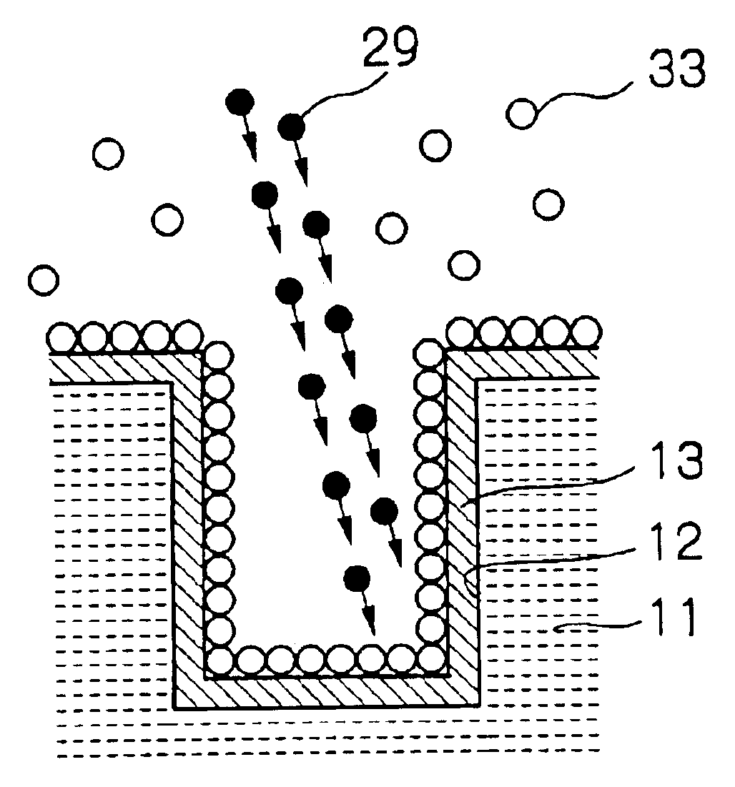
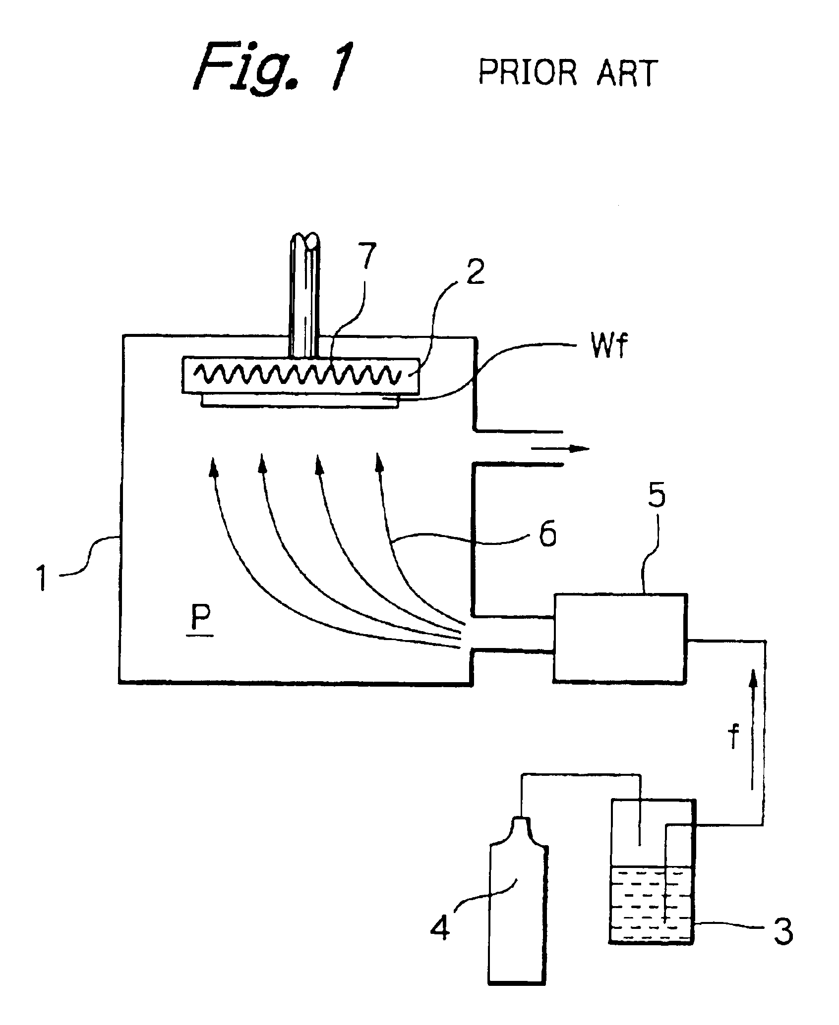
[0105]FIG. 9 is a schematic diagram illustrating an exemplary configuration of a coating apparatus of CVD technology according to the present invention. In FIG. 9, reference numeral 21 designates a reaction chamber which has a susceptor 22 arranged therein for loading / holding a substrate Wf thereon, and an exhaust port 32 of the reaction chamber 21 is connected to a vacuum evacuation system equipped with a vacuum pump or the like so as to be decompressed to a specified pressure. Reference numeral 23 designates a source container for containing a liquid source, from which the liquid source is sent to a vaporizer 26 by supplying H2 gas from an H2 reservoir 24 via a flow controller 25 to the source container 23, so as to be vaporized in the vaporizer 26 and then to be supplied into the reaction chamber 21 as a source gas 27.

[0106]Reference numeral 28 designates a...


PUM

PropertyMeasurementUnit
particle energyaaaaaaaaaa
temperatureaaaaaaaaaa
roughnessaaaaaaaaaa

Abstract

There is provided a method of performing a surface treatment, such as coating, denaturation, modification and etching, on a surface of a substrate. The method comprises the steps of bringing a surface treatment gas into contact with a surface of a substrate, and irradiating the surface of the substrate with a fast particle beam to enhance an activity of the surface and/or the surface treatment gas, thereby facilitating a reaction between the surface and the gas. The fast particle beam may be selected from a group consisting of an electron beam, a charged particle beam, an atomic beam and molecular beam. For example, during a coating operation, chemical deposition of predetermined component elements of the gas onto the surface is effected and a predetermined portion of the surface of the substrate is irradiated with a particle beam to form a coating layer on the predetermined portion.

Description

BACKGROUND OF THE INVENTION[0001]The present invention relates to a surface treatment technology including coating, modification and etching of a surface of a substrate (such as a semiconductor wafer), in particular, to a surface treatment technology using various kinds of beams, such as particle beams, for facilitating reaction of the surface to a source material used in the surface treatment.[0002]With rapid achievement of finer and even more densely packed semiconductor devices, an interconnect (or circuit wiring) pitch has become markedly narrow, and an interconnect electric density has increased considerably. As a result, conventional semiconductor devices comprising an interlayer insulative film layer of silicon oxide and an aluminum-based conductor are confronted with serious problems, i.e. an RC delay phenomenon in signal transmission (i.e. a delay relating to electrical resistance and static capacitance) and electro-migration damage to conductor material. To solve such a pr...

Claims


Application Information

Patent Timeline
Patent Type & Authority Patents(United States)
IPC IPC(8): C23C16/18C23C16/448C23C16/48C23C16/452H01J37/32H01L21/285H01L21/02H01L21/3213
CPCC23C16/18C23C16/452C23C16/486C23C16/487H01J37/3233H01J37/32422H01L21/28556H01L21/32136
Inventor OGURE, NAOAKIHORIE, KUNIAKIARAKI, YUJINAGASAKA, HIROSHIKAKUTANI, MOMOKOSATAKE, TOHRU
Owner EBARA CORP
Why Eureka
Try Eureka