Graded thin films

a thin film, grade technology, applied in the direction of chemical vapor deposition coating, crystal growth process, coating, etc., can solve the problems of extremely thin silicon dioxide gate dielectrics, electrons exhibit a finite probability of crossing the barrier, and conventional gate oxide layers may be inadequate in several respects

Inactive Publication Date: 2005-08-23
ASM INTERNATIONAL
View PDF34 Cites 148 Cited by
  • Summary
  • Abstract
  • Description
  • Claims
  • Application Information

AI Technical Summary

Benefits of technology

[0021]Due to the fine control provided by atomic layer deposition, this grading can be provided in very thin layers. Moreover, the low temperatures during the process enables maintenance of the desired impurity content profile.

Problems solved by technology

Conventional gate oxide layers may be inadequate in several respects as dimensions are continuously scaled.
Extremely thin silicon dioxide gate dielectrics exhibit undesirable phenomena such as quantum-mechanical tunneling.
However, the electron exhibits a finite probability of crossing the barrier even if the electron does not possess sufficient kinetic energy.
Another problem with thin gate oxides is their susceptibility to dopant diffusion from the overlying gate electrode.
As the gate oxide thickness is scaled down, boron can easily penetrate through the gate oxide, resulting in instabilities in device properties.
Boron penetration into gate dielectrics has such undesirable consequences as positive shifts in threshold voltage, increases in sub-threshold swing, increases in charge trapping, decreases in low-field hole mobility, and degradation of current drive due to polysilicon depletion in p-MOSFETs.
However, the interfaces between silicon nitride films and the underlying semiconductor substrate are generally of poor quality, resulting in a high density of charge trapping sites and pinholes, and attendant current leakage.
Conventional methods of incorporating nitrogen into silicon oxide gate dielectrics are difficult to control, however, particularly for ultra-thin gate dielectrics of future generation devices
While exhibiting greatly increased dielectric strength, these materials have been difficult to integrate with existing fabrication technology.
Another issue raised by the continual scaling of integrated circuit dimensions is the difficulty of producing adequately conductive metal lines for wiring the circuitry within integrated circuits.
Unfortunately, scaling introduces difficulties with damascene processes, particularly when fast diffusing metals like copper are employed for the metal lines and contacts.
These lining layers occupy a considerable volume of the available trenches, reducing room available for the more highly conductive metal filler.
Moreover, employing metal nitride liners, though advantageously containing the metal filler and preventing short circuits, has been known to induce electromigration during circuit operation, leading to voids and further reduced conductivity along the metal lines.

Method used


Image

  • Graded thin films
  • Graded thin films
  • Graded thin films

Examples


second embodiment

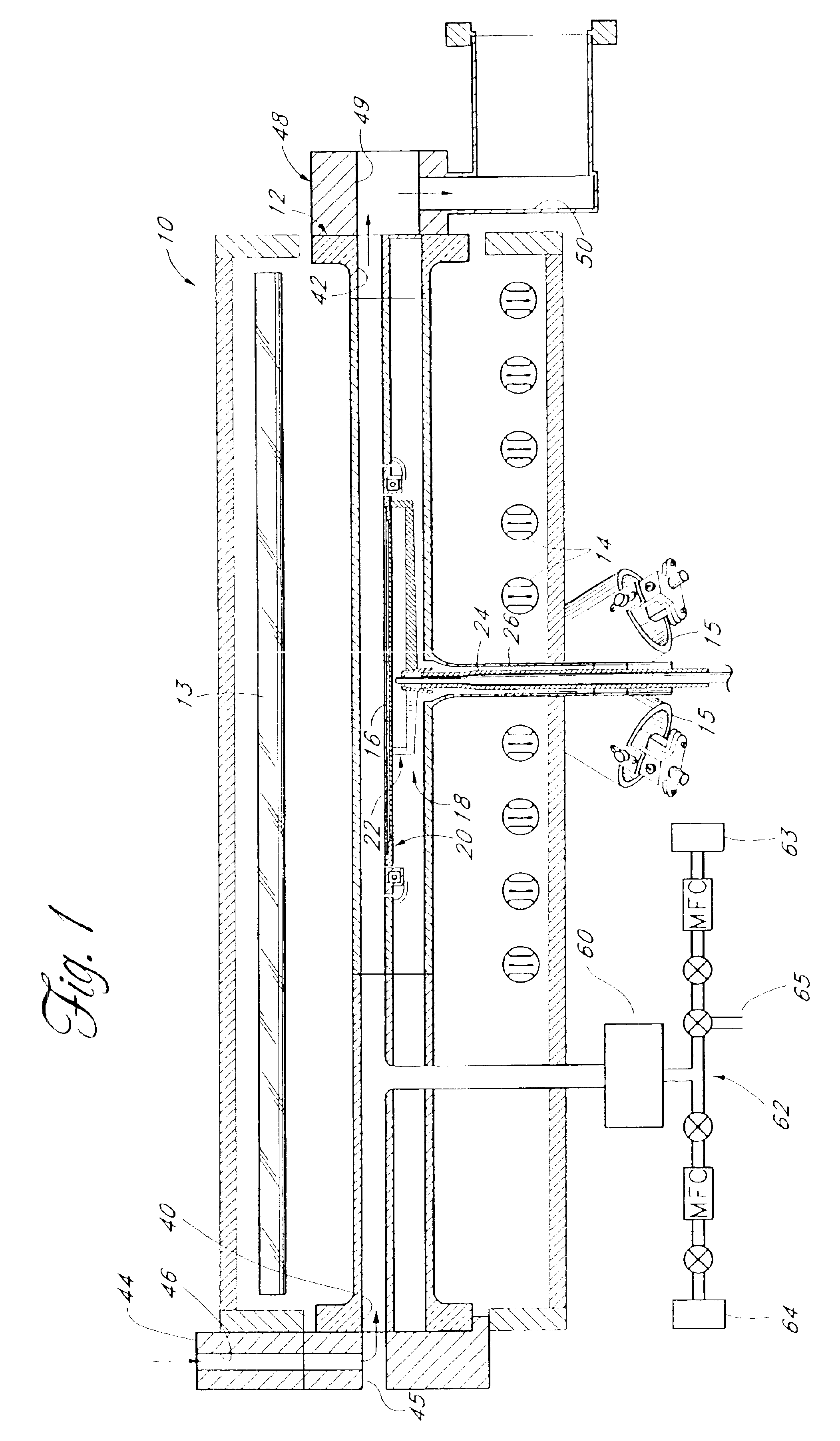
[0045]For the first illustrated embodiment, gas sources include tanks holding a silicon-containing gas, preferably a silane such as monosilane (SiH4), silicon tetrachloride (SiCl4), dichlorosilane (DCS or SiH2Cl2), trichlorosilane (TCS or SiHCl3), or other silane or halosilane silicon sources; an oxidant source gas, such as O2, O3, O radicals, H2O, NO or N2O; and a nitrogen source gas, such as NH3. Metal source gases can also be employed for deposition of high k metal oxides. For the second embodiment, source gases include one or more metal source gases (e.g., WF6, TiCl4, CuCl, etc.), a nitrogen source gas (e.g., NH3) and a reducing agent (e.g., triethyl boron or TEB).

[0046]The silicon sources can include a bubbler and a gas line for bubbling H2 through a liquid solution such as TCS, to more effectively transport silicon-containing gas molecules to the reaction chamber in gaseous form. Many metal sources can similarly include liquid solutions and bubblers. The reactor 10 can also in...

first embodiment

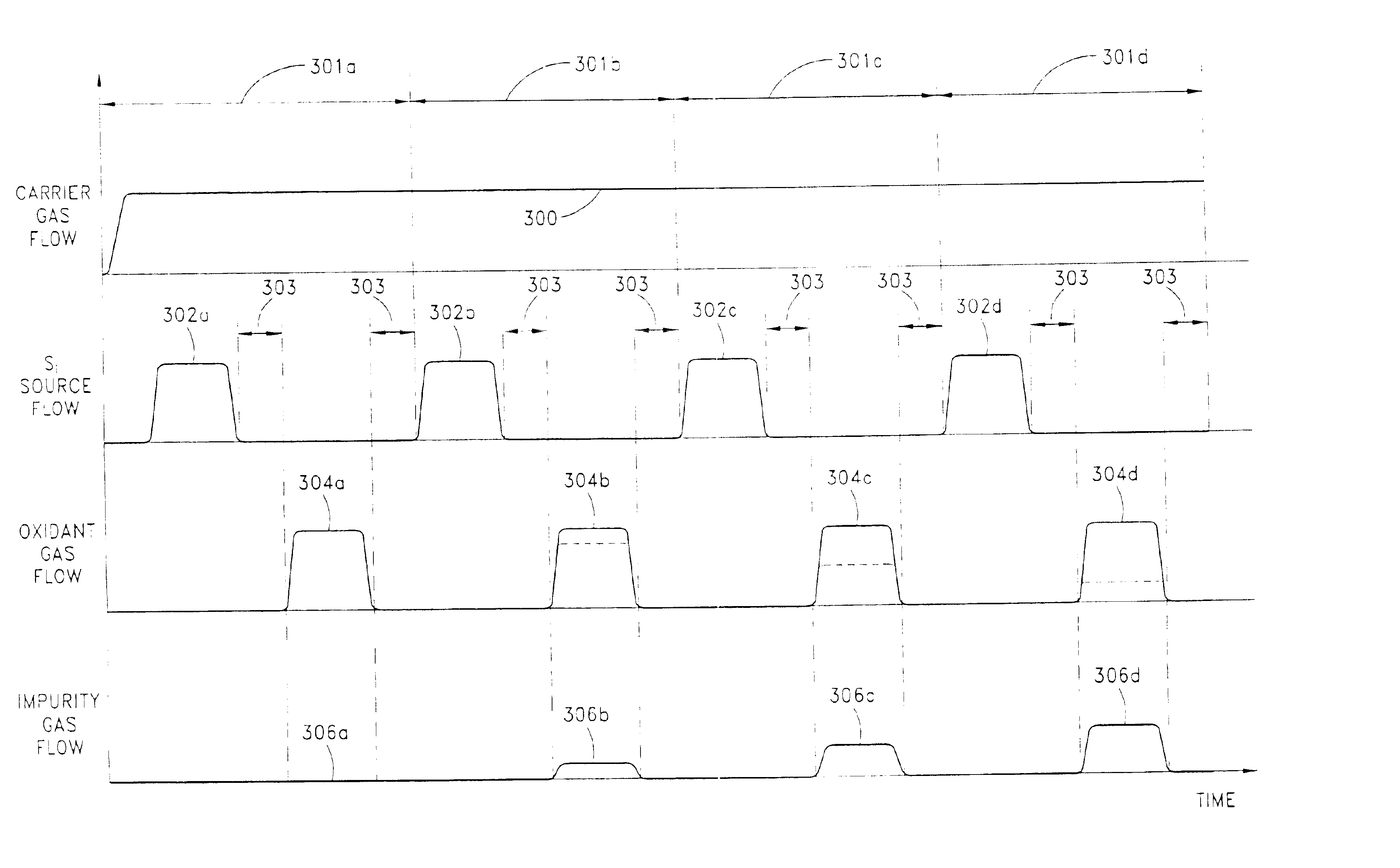
[0053]The first embodiment involves alternating adsorption of no more than about a monolayer of silicon with oxidation of the previously adsorbed monolayer in an alternating layer silicon oxide process. During the oxidation stage, nitrogen can also be selectively incorporated. Essentially, by mixing these two gases, oxynitride films with any desired ratio of oxygen to nitrogen can be grown. In the preferred embodiment, varying reactant ratios during the cyclical process, the composition formed by each cycle can be tailored. Most preferably, the deposition begins with pure silicon oxide and ends with pure silicon nitride, with any desired grading through the thickness.

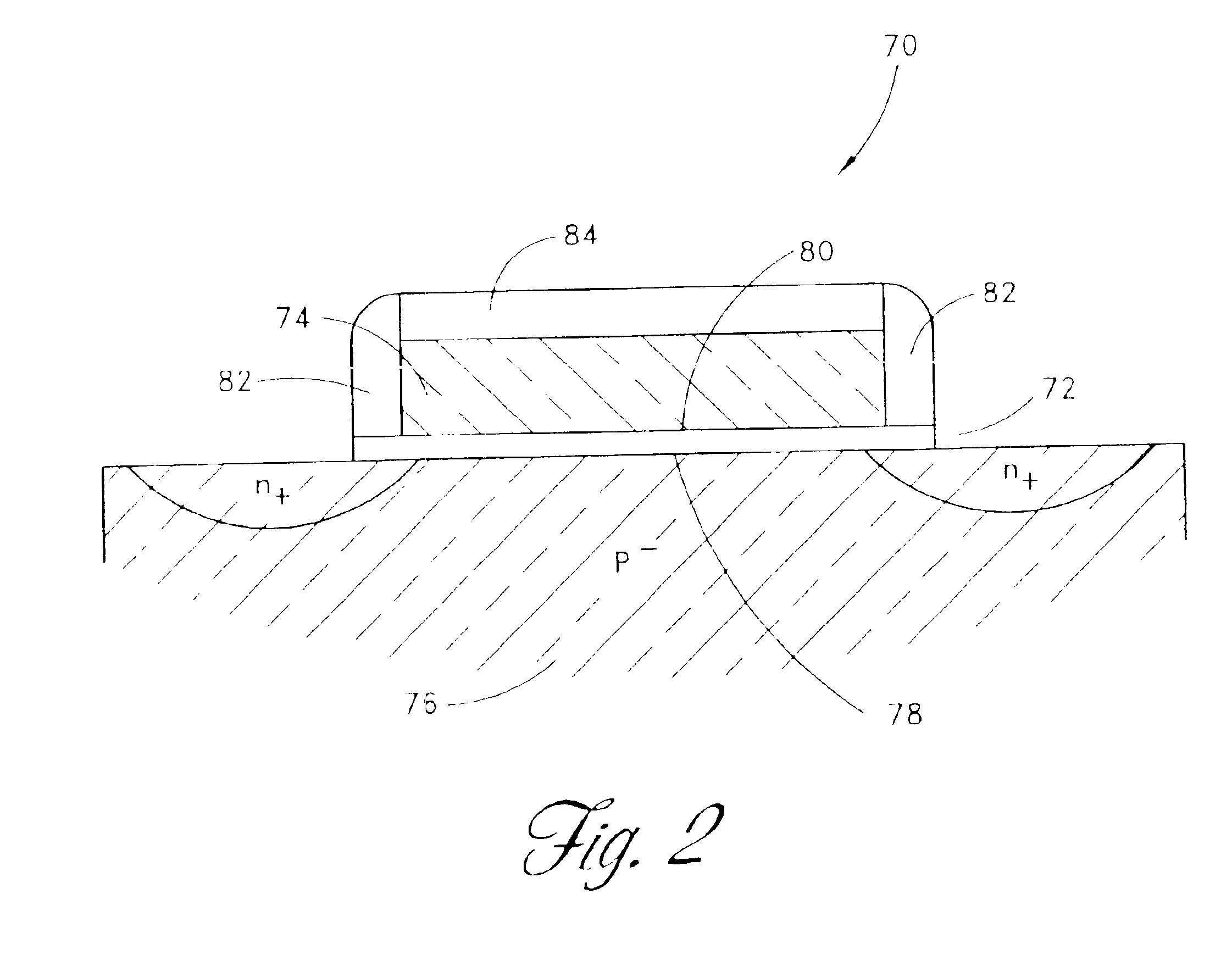
[0054]The substrate upon which deposition is to occur is initially prepared for the self-limiting deposition process. In the illustrated embodiment, the substrate is a semiconductor material in which a transistor channel is formed. The semiconductor substrate can be formed of an epitaxial layer or formed of the top port...


PUM

PropertyMeasurementUnit
widthsaaaaaaaaaa
thicknessesaaaaaaaaaa
pressureaaaaaaaaaa

Abstract

Thin films are formed by atomic layer deposition, whereby the composition of the film can be varied from monolayer to monolayer during cycles including alternating pulses of self-limiting chemistries. In the illustrated embodiments, varying amounts of impurity sources are introduced during the cyclical process. A graded gate dielectric is thereby provided, even for extremely thin layers. The gate dielectric as thin as 2 nm can be varied from pure silicon oxide to oxynitride to silicon nitride. Similarly, the gate dielectric can be varied from aluminum oxide to mixtures of aluminum oxide and a higher dielectric material (e.g., ZrO2) to pure high k material and back to aluminum oxide. In another embodiment, metal nitride (e.g., WN) is first formed as a barrier for lining dual damascene trenches and vias. During the alternating deposition process, copper can be introduced, e.g., in separate pulses, and the copper source pulses can gradually increase in frequency, forming a graded transition region, until pure copper is formed at the upper surface. Advantageously, graded compositions in these and a variety of other contexts help to avoid such problems as etch rate control, electromigration and non-ohmic electrical contact that can occur at sharp material interfaces.

Description

REFERENCE TO RELATED APPLICATION[0001]This application is a continuation of U.S. patent application Ser. No. 09 / 800,757, filed Mar. 6, 2001, now U.S. Pat. No. 6,534,355, which claims the priority benefit of U.S. Provisional Application Ser. No. 60 / 187,423, filed Mar. 7, 2000.FIELD OF THE INVENTION[0002]The present invention relates generally to forming layers in integrated circuits, and more particularly to depositing thin films with graded impurity concentrations.BACKGROUND OF THE INVENTION[0003]There are numerous semiconductor process steps involved in the development of modem day integrated circuits (ICs). From the initial fabrication of silicon substrates to final packaging and testing, integrated circuit manufacturing involves many fabrication steps, including photolithography, doping, etching and thin film deposition. As a result of these processes, integrated circuits are formed of microscopic devices and wiring amid multiple layers.[0004]A basic building block of the integra...

Claims


Application Information

Patent Timeline
Patent Type & Authority Patents(United States)
IPC IPC(8): C23C16/02C30B25/14C23C16/455H01L21/02H01L21/28H01L21/285H01L21/70H01L21/318H01L21/768H01L21/314H01L29/51H01L21/316H01L29/40C23C16/40C23C16/48C23C16/44C23C16/34C23C16/30
CPCC23C16/029C23C16/401C23C16/403C23C16/405C23C16/452C23C16/45529C23C16/45531C23C16/45534C30B25/14H01L21/0214H01L21/02178H01L21/02189H01L21/02194H01L21/02211H01L21/02274H01L21/0228H01L21/28185H01L21/28194H01L21/28202H01L21/28562H01L21/3141H01L21/3145H01L21/31612H01L21/3162H01L21/31641H01L21/3185H01L21/76846H01L21/76873H01L21/76879H01L29/513H01L29/517H01L29/518H01L29/4908C23C16/34Y10T428/2495H01L2221/1089H01L2924/0002Y10T428/24942H01L2924/00H01L21/02142
Inventor WERKHOVEN, CHRISTIAAN J.RAAIJMAKERS, IVOHAUKKA, SUVI P.
Owner ASM INTERNATIONAL
Why Eureka
Try Eureka