High density non-volatile memory device

a non-volatile, high-density technology, applied in the field of memory devices, can solve the problems of unsuitable molecular memory use, inability to meet the requirements of molecular memory, and intrinsic diffraction-limited size constraints of light-mediated data storage, and achieve the effect of preventing charge leakage and suitability mechanical properties

Inactive Publication Date: 2006-05-09
NORTH CAROLINA STATE UNIV +1
View PDF51 Cites 31 Cited by
  • Summary
  • Abstract
  • Description
  • Claims
  • Application Information

AI Technical Summary

Benefits of technology

[0041]The term “storage medium” refers to a composition comprising two or more storage molecules. The storage medium can contain only one species of storage molecule or it can contain two or more different species of storage molecule. In preferred embodiments, the term “storage medium” refers to a collection of storage molecules. Preferred storage media comprise a multiplicity (at least 2) of different and distinguishable (preferably non-neutral) oxidation states. The multiplicity of different and distinguishable oxidation states can be produced by the combination of different species of storage molecules, each species contributing to said multiplicity of different oxidation states and each species having a single non-neutral oxidation state. Alternatively or in addition, the storage medium can comprise one or more species of storage molecule having a multiplicity of non-neutral oxidation states. The storage medium can contain predominantly one species of storage molecule or it can contain a number of different storage molecules. The storage media can also include molecules other than storage molecules (e.g. to provide chemical stability, suitable mechanical properties, to prevent charge leakage, etc.).

Problems solved by technology

While these approaches generally employ molecular architectures that can be switched between two different states, all of the approaches described to date have intrinsic limitations making their uses in computational devices difficult or impractical.
Each of these approaches, however, has intrinsic limitations that ultimately render it unsuitable for use in molecular memories.
Light-mediated data storage has intrinsic diffraction-limited size constraints.
Moreover, most photochromic schemes are limited to scanning and interrogating dyes deposited on a surface and are not amenable to 3-D data storage.
In addition, it is noted that these dyes often exhibit relatively slow switching times ranging from microsecond to millisecond durations.
Quite high fields (>107 V / cm) must be applied to observe an altered absorption spectrum which can result in heat / power dissipation problems.
In addition, the change in the absorption spectrum is typically quite small, which can present detection difficulties.
The latter requirement may be difficult to achieve on a solid substrate.
Furthermore, any optical reading scheme would pose the same 2-D limitations as described for photochromic dyes.
The chemically induced systems have applications as sensors but are not practical for memory storage, while the photochemically induced systems have the same fundamental limitations as photochromic dyes.
Moreover, methods have not yet been developed for delineating the conformation / structure of the molecular machine that are practical in any device applications.
1H NMR spectroscopy, for example, is clearly the method of choice for elucidating structure / conformation for molecules in solution, but is totally impractical for interrogating a molecular memory element.
None of the current architectures for molecular machines has been designed for assembly on a solid substrate, an essential requirement in a viable device.
In summary, photochromic dyes, electrochromic dyes, redox-sensitive dyes, and molecular machines all have fundamental limitations that have precluded their application as viable memory elements.
These molecular architectures are typically limited by reading / writing constraints.
Furthermore, even in cases where the effective molecular bistability is obtained, the requirement for photochemical reading restricts the device architecture to a 2-dimensional thin film.
Such limitations greatly diminish the appeal of these devices as viable molecular memory elements.

Method used


Image

  • High density non-volatile memory device
  • High density non-volatile memory device
  • High density non-volatile memory device

Examples


example 1

Thiol-Porphyrins for Attachment to Electroactive Surfaces as Molecular Memory Devices

I. Molecular Design

[0330]This example presents the design and synthesis of porphyrins that can be attached covalently, in defined geometries, to electroactive surfaces. For the present purposes, we consider only the surface of a gold electrode. Three design features we sought to obtain included the following: (1) The ability to attach porphyrins via a sulfide linkage to the gold electrode surface with the porphyrins oriented vertically or horizontally. (2) The ability to tune the porphyrin electrochemical oxidation potential through the use of electron-withdrawing or releasing substituents at the periphery of the porphyrin, or the use of different metals in metalloporphyrins. (3) The use of thiol protecting groups that would cleave spontaneously on the gold surface, thereby avoiding the potential practical problems of handling free thiols.

[0331]In order to achieve a vertical orientation of the porph...

example 2

Setting and Reading the State of a Porphyrinic Macrocycle

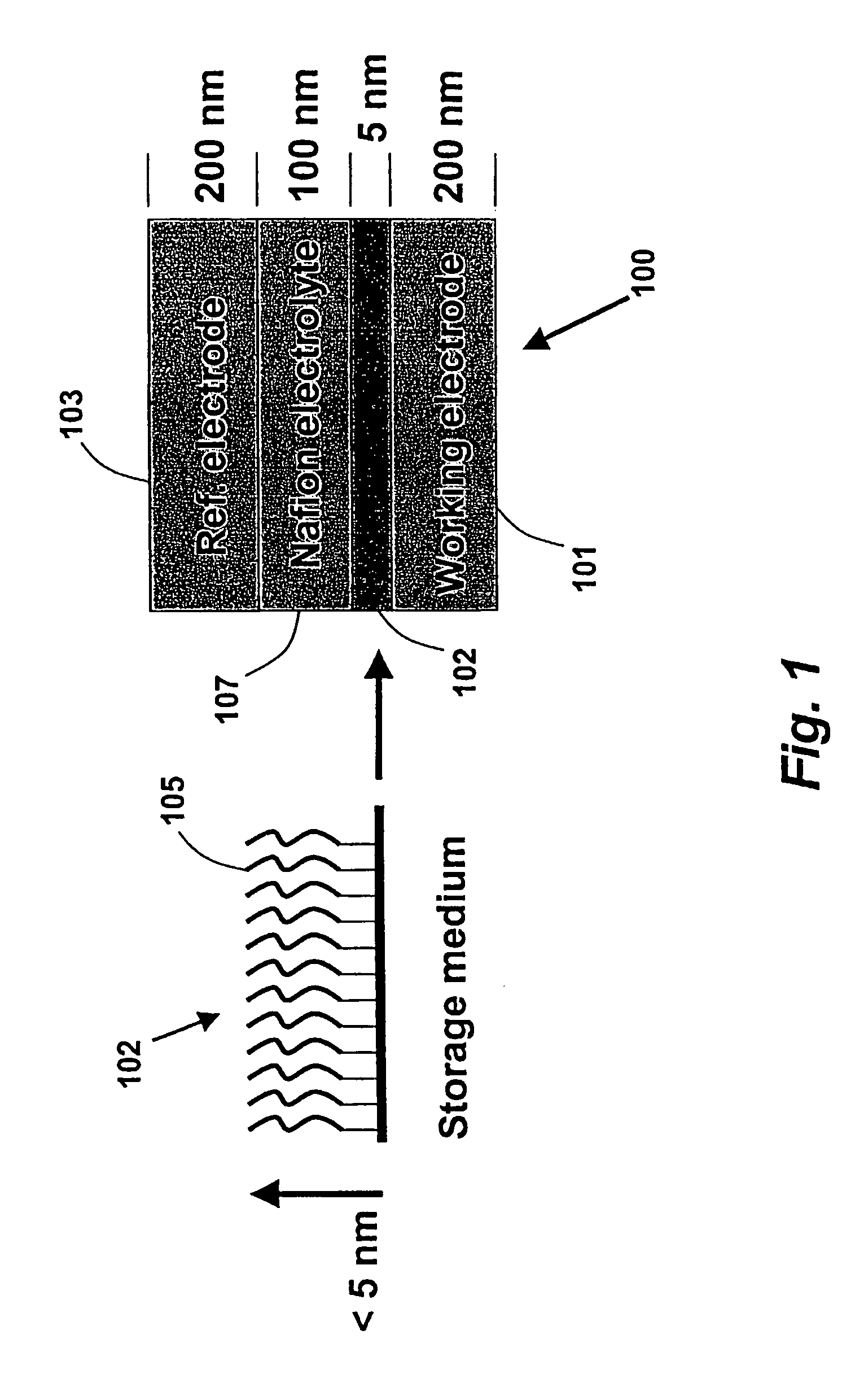
1. Preparation of Gold Electrodes, Formation of Electrochemical Cell, Deposition of Thiol-Porphyrin Monolayer.

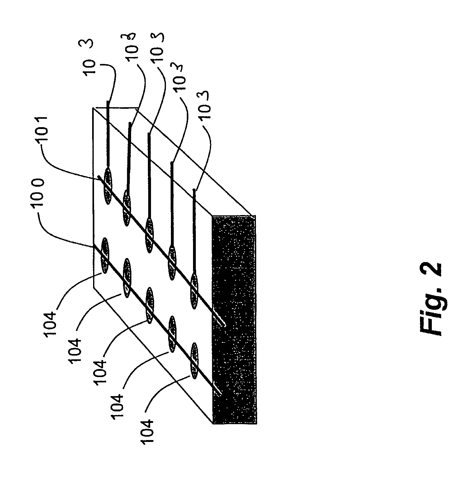
[0396]Glass slides were soaked in 90° C. piranha solution for thirty minutes, thoroughly rinsed with doubly distilled water, and dried under vacuum. A 1 nm layer of chromium was evaporated onto the glass, followed by 100 nm of gold through a thin mask consisting of four parallel lines, each with a width of approximately 75 microns, spaced at approximately 1 mm intervals. All depositions were done at 10−6 torr using an E-beam evaporator.

[0397]Immediately after venting of the vacuum system, the slides were removed and stored under dry ethanol until use. The slides were dried with a stream of nitrogen and a piece of PDMS with a 3 mm diameter hole in the center was immediately placed over all four gold electrodes and filled with a porphyrin solution (0.1 mg per milliliter in dry ethanol) (Z-15 from example 1).

[0398]The sli...

example 3

Tightly Coupled Porphyrin Arrays for Molecular Memory Storage

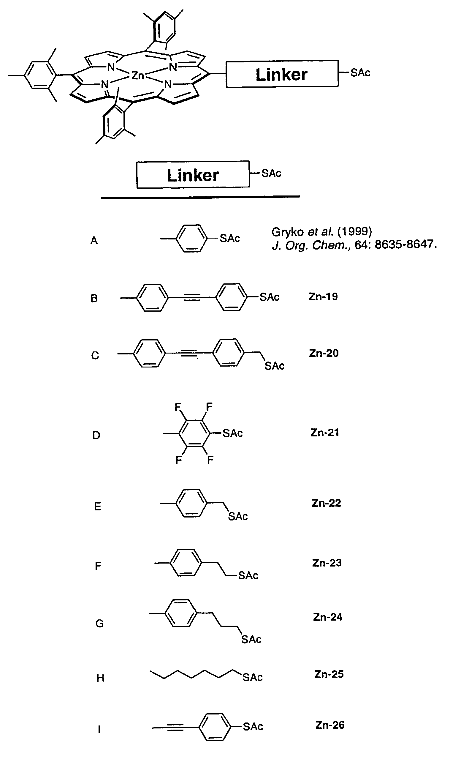
[0404]We have been developing approaches for molecular-based information storage where information is stored in the different oxidation states of molecular porphyrin arrays. To explore a simple design for suitable storage molecules, we report here the synthesis of porphyrin arrays where porphyrins, having identical oxidation potentials, are directly linked to one another instead of joined via a molecular linker. Oxidative coupling with AgPF6 of zinc(II)-5,15-bis(4-tert-butylphenyl)-10-phenylporphyrin, obtained by a rational synthesis, afforded the expected meso,meso-linked dimer and an unexpected meso,meso,meso-linked trimer. For attachment to an electroactive surface we synthesized a meso,meso-linked porphyrin dimer with a thiol-linker in one of the meso-positions. The thiol-group was protected as thioacetyl moiety to avoid handling of free thiol groups. Coupling of zinc(II)-5,10,15-tris(3,5-di-tert-butylphenyl)porphyrin ...


PUM

PropertyMeasurementUnit
voltageaaaaaaaaaa
voltageaaaaaaaaaa
voltageaaaaaaaaaa

Abstract

This invention provides novel high density memory devices (FIG. 3) that are electrically addressable permitting effective reading and writing, that provide a high memory density (102), that provide a high degree of fault tolerance, and that are amenable to efficient chemical synthesis and chip fabrication. The devices arc intrinsically latchable, defect tolerant, and support destructive or non-destructive read cycles. In a preferred embodiment, the device comprises a fixed electrode electrically coupled to a storage medium having a multiplicity of different and distinguishable oxidation states wherein data is stored in said oxidation states by the addition or withdrawal of one or more electrons from said storage medium via the electrically coupled electrode.

Description

CROSS-REFERENCE TO RELATED APPLICATION[0001]This application is a filing under 35 U.S.C. §371 of PCT application PCT / US00 / 17847, filed on Jun. 28, 2000, which is a CIP of U.S. Ser. No. 09 / 346,221, filed on Jul. 1, 1999 now U.S. Pat. No. 6,208,553, and Ser. No. 09 / 484,394, filed on Jan. 14, 2000 U.S. Pat. No. 6,324,091 & Ser. No. 09 / 346,228 Jul. 1, 1999 now U.S. Pat. No. 6,381,169, all of which are incorporated herein by reference in their entirety for all purposes.STATEMENT AS TO RIGHTS TO INVENTIONS MADE UNDER FEDERALLY SPONSORED RESEARCH AND DEVELOPMENT[0002]This invention was made with government support under Grant Number N00014-99-1-0357 from the Office of Naval Research. The Government of the United States of America may have certain rights in the invention.FIELD OF THE INVENTION[0003]This invention relates to memory devices. In particular this invention provides a nonvolatile electronic memory device capable of storing information in extremely high density.BACKGROUND OF THE I...

Claims


Application Information

Patent Timeline
Patent Type & Authority Patents(United States)
IPC IPC(8): G11C7/00H01L21/8247C07D487/22C07D519/00C07F17/02G11C11/00G11C11/56G11C13/02H01L27/115H01L27/28H01L51/30
CPCB82Y10/00H01L51/0595C07D487/22C07D519/00C07F17/02G11C11/5664G11C13/0009G11C13/0014G11C13/0016G11C13/0069H01L27/28H01L51/0077H01L51/0078H01L51/0084B82Y30/00G11C13/025G11C2013/009G11C2213/15G11C2213/77H01L51/009G11B9/14G11B9/149H10K85/311H10K85/30H10K85/341H10K85/361H10K10/701H10K19/00
Inventor BOCIAN, DAVID F.KUHR, WERNER G.LINDSEY, JONATHANCLAUSEN, PETER CHRISTIANGRYKO, DANIEL TOMASZ
Owner NORTH CAROLINA STATE UNIV
Why Eureka
Try Eureka