Monolithic integration of enhancement- and depletion-mode AlGaN/GaN HFETs

a heterojunction field effect transistor and enhancement-depletion-mode technology, applied in the direction of transistors, semiconductor devices, electrical apparatus, etc., can solve the problems of poor performance characteristics of e-mode hfets fabricated in this manner, low transconductance, large on-resistance, etc., to achieve low knee-voltage, low extrinsic transconductance, and low on-resistance

Active Publication Date: 2011-07-05
THE HONG KONG UNIV OF SCI & TECH
View PDF55 Cites 35 Cited by
  • Summary
  • Abstract
  • Description
  • Claims
  • Application Information

AI Technical Summary

Benefits of technology

Group III-nitride (“III-N”) compound semiconductors, such as those incorporating AlGaN / GaN, possess the advantages of having wide bandgap, high breakdown field, and large thermal conductivity, which can bring significant benefits to the design of heterostructure field-effect transistors and applications utilizing HFETs. Because of their high power handling capabilities, AlGaN / GaN HFETs can be used for radio frequency / microwave power amplifiers and high power switches. However, most power amplifiers and switches using AlGaN / GaN HFETs feature depletion-mode (“D-mode”) HFETs as the building block. Since a D-mode HFET is a transistor with a negative value for the threshold voltage (Vth), D-mode HFETs need both a positive and negative voltage bias to be turned on and off. If an enhancement-mode (“E-mode”) HFET could be made available, only a positive voltage supply would be needed for circuit applications, resulting in simplified circuits and reduced costs.
Another attempt to fabricate an E-mode HFET in an AlGaN / GaN system was reported by Hu et al., “Enhancement mode AlGaN / GaN HFET with selectively grown PN junction gate,” April 2000, IEE Electronics Letters, Vol. 36, No. 8, pp. 753-754, which is hereby incorporated by reference in its entirety. In this work a selectively-grown P / N junction gate is used. The selectively-grown P-type layer is able to raise the potential of the channel and therefore deplete the carriers from the channel at zero gate bias. However, such an approach is not self-aligned and the problem of large access resistance persists.
The disclosed innovations in various embodiments, provide one or more of at least the following advantages:Allows for monolithic integration of enhancement-mode and depletion-mode AlGaN / GaN HEMTs for the implementation of complete circuits in DCFL or other logic families.Provides a self-aligned approach to fabricating E / D-mode AlGaN / GaN HEMTs with low on-resistance, low knee-voltage, and high extrinsic transconductance.Provides a method to manufacture self-aligned E / D-mode HFETs using readily available microelectronic fabrication equipment.Provides a method enabling the production of reproducible and stable E / D-mode HEMT devices, particularly suitable for high temperature digital circuit applications.Provides for allowing large supply voltage in DCFL circuit to improve the noise margin and to shorten gate delay.Provides for large input voltage swings to eliminate the need for logic level adjustment between adjacent stages in IC's.Provides a planar integration for E / D-mode HEMTs without any mesa etching or gate recess etching.

Problems solved by technology

However, E-mode HFETs fabricated in this manner have poor performance characteristics, such as low transconductance, large on-resistance, and high knee-voltage.
Note that gates that are not self-aligned required overlap, which increases device size and stray capacitance.
However, such an approach is not self-aligned and the problem of large access resistance persists.
However, ICP-RIE can cause serious damage to the AlGaN barrier and results in increased gate leakage current.
Thus, the gate patterns have to be created again through photo-lithography which cannot be accurately aligned with the recess-etching windows previously generated in the gate recess stage.
Another problem associated with the ICP-RIE etching is the poor uniformity in the etching depth, which is undesirable for integrated circuits because it severely affects the uniformity in the threshold voltage.
However, in an AlGaN / GaN HFET, because of the lack of effective wet etching techniques, the recess etching is carried out by dry etching.
For example, ICP-RIE is used for the recess etching, as mentioned earlier, with the accompanying severe damage and defects to the device.
However, no metal has been found to have a work function larger than 1 electron volt (“eV”).
This is not suitable for the integration of E-mode and D-mode HEMTs, which are both required for DCFL circuits.
As described above, such approach requires a two-mask gate process, introducing extra process steps and cost as compared to a single-mask gate process.
Additionally, due to the lack of P-channel AlGaN / GaN HEMTs, a circuit configuration similar to the based on CMOS cannot be implemented at present.

Method used


Image

  • Monolithic integration of enhancement- and depletion-mode AlGaN/GaN HFETs
  • Monolithic integration of enhancement- and depletion-mode AlGaN/GaN HFETs
  • Monolithic integration of enhancement- and depletion-mode AlGaN/GaN HFETs

Examples


example 1

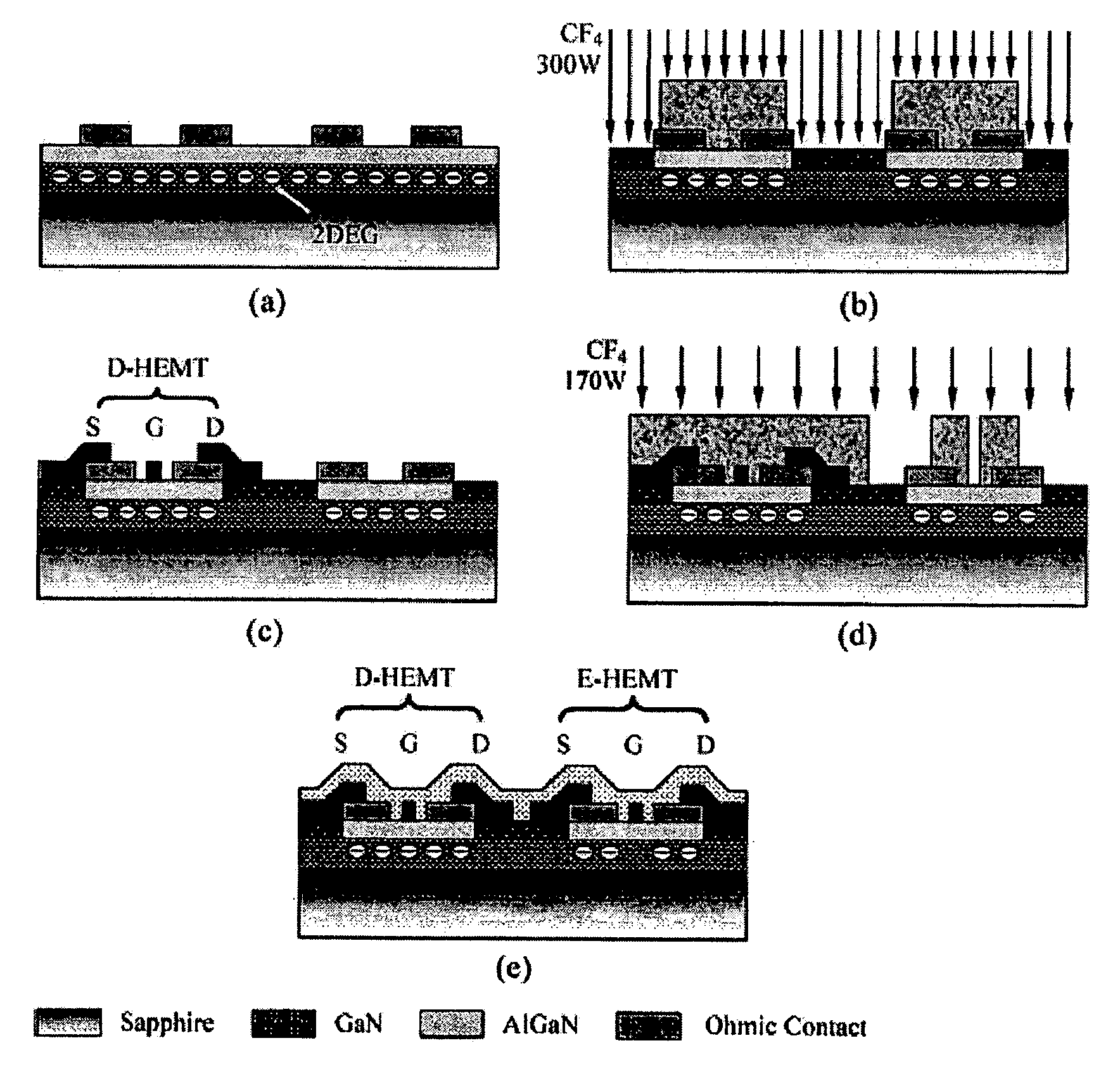
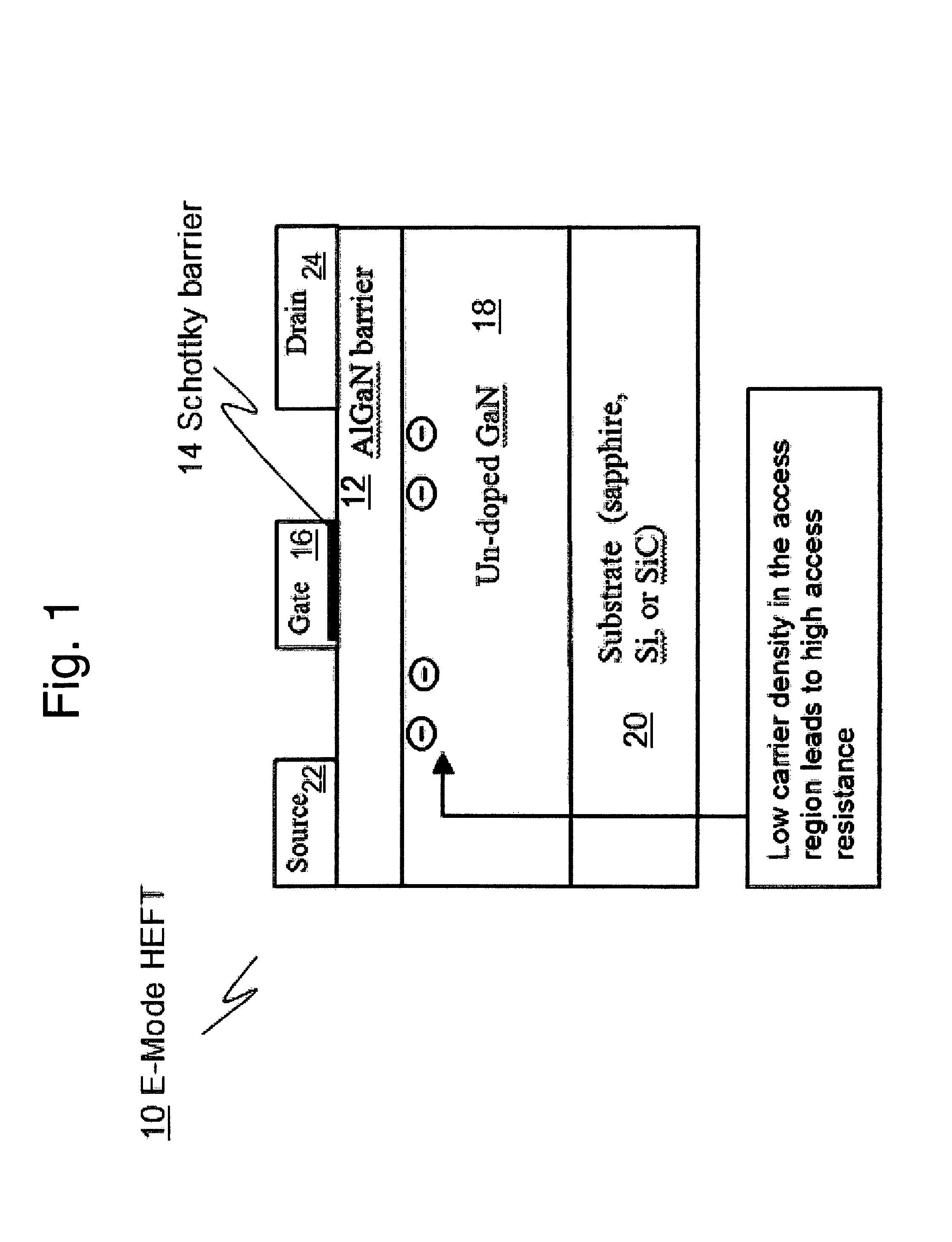
An AlGaN / GaN HEMT structure was grown on a (0001) sapphire substrate in an Aixtron AIX 2000 HT metal-organic chemical vapor deposition (MOCVD) system. The HEMT structure consists of a low-temperature GaN nucleation layer, a 2.5-m-thick unintentionally doped GaN buffer layer and an AlGaN barrier layer with nominal 30% Al composition. The barrier layer consists of a 3-nm undoped spacer, a 15-nm carrier supplier layer doped at 2.5×1018 cm−3, and a 2-nm undoped cap layer. Room temperature Hall measurements of the structure yield an electron sheet density of 1.3×1013 cm−2 and an electron mobility of 1000 cm2 / Vs. The device mesa was formed using Cl2 / He plasma dry etching in an STS ICP-RIE system followed by the source / drain ohmic contact formation with Ti / Al / Ni / Au annealed at 850° C. for 45 seconds. The ohmic contact resistance was typically measured to be 0.8 ohm-mm.

After gate windows with 1 nm length were opened by contact photolithography, the sample was treated by CF4 plasma in an RIE...

example

DCFL Ring Oscillator

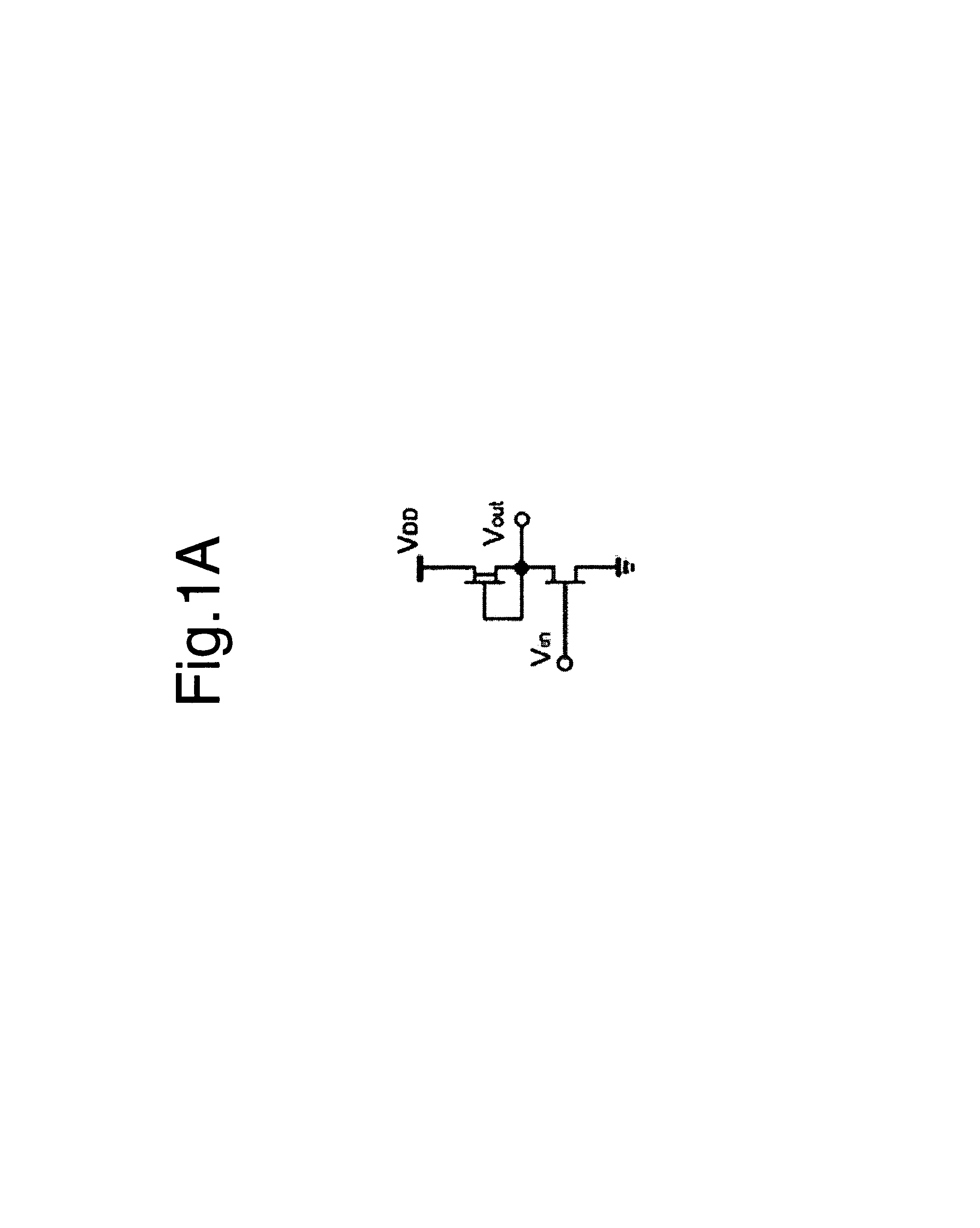
FIG. 1B shows a schematic circuit diagram of a DCFL ring oscillator, which is formed with an odd-numbered E / D inverter chain. Seventeen-stage ring oscillators were fabricated with inverters' β=6.7, 10, and 25. For each ring oscillator, 36 transistors were used including an output buffer. FIG 1D shows a photomicrograph of a fabricated ring oscillator according to the present innovations. The ring oscillator were characterized on-wafer using an Agilent E4404B spectrum analyzer and an HP 54522A oscilloscope. The DC power consumption was also measured during the ring oscillators' operation. FIGS. 44 and 45 show the frequency- and time-domain characteristics of the 17-stage ring oscillator with β=10 biased at VDD=3.5 V. The fundamental oscillation frequency is 225 MHz. According to the formula of propagation delay per stage τpd=(2nf)−1, where the number of stages n is 17, and τpd was calculated to be 130 ps / stage. The dependences of τpd and power-delay product on VDD ...


PUM


Abstract

A method for and devices utilizing monolithic integration of enhancement-mode and depletion-mode AlGaN / GaN heterojunction field-effect transistors (HFETs) is disclosed. Source and drain ohmic contacts of HFETs are first defined. Gate electrodes of the depletion-mode HFETs are then defined. Gate electrodes of the enhancement-mode HFETs are then defined using fluoride-based plasma treatment and high temperature post-gate annealing of the sample. Device isolation is achieved by either mesa etching or fluoride-based plasma treatment. This method provides a complete planar process for GaN-based integrated circuits favored in high-density and high-speed applications.

Description

BACKGROUND AND SUMMARY OF THE INVENTIONThe present application relates to a method for monolithic integration of enhancement and depletion-mode heterojunction field effect transistors (“HFETs”) , and in particular, to fabrication of aluminum-gallium nitride / gallium nitride (“AlGaN / GaN”) HFETs using such monolithic integration.Group III-nitride (“III-N”) compound semiconductors, such as those incorporating AlGaN / GaN, possess the advantages of having wide bandgap, high breakdown field, and large thermal conductivity, which can bring significant benefits to the design of heterostructure field-effect transistors and applications utilizing HFETs. Because of their high power handling capabilities, AlGaN / GaN HFETs can be used for radio frequency / microwave power amplifiers and high power switches. However, most power amplifiers and switches using AlGaN / GaN HFETs feature depletion-mode (“D-mode”) HFETs as the building block. Since a D-mode HFET is a transistor with a negative value for the t...

Claims


Application Information

Patent Timeline
Patent Type & Authority Patents(United States)
IPC IPC(8): H01L21/338
CPCH01L21/8252H01L27/0605H01L29/66462H01L29/7787H01L29/2003
Inventor CHEN, JINGCAI, YONGLAU, KEI MAY
Owner THE HONG KONG UNIV OF SCI & TECH
Why Eureka
Try Eureka