Microbolometer and preparation method thereof

A technology of microbolometer and microbridge, which is applied in the field of microbolometer and its preparation, can solve the problems of complex composition, poor stability of film chemical structure, and low sensitivity of pyroelectric detectors

Inactive Publication Date: 2010-07-14
UNIV OF ELECTRONICS SCI & TECH OF CHINA
View PDF3 Cites 28 Cited by
  • Summary
  • Abstract
  • Description
  • Claims
  • Application Information

AI Technical Summary

Problems solved by technology

However, since the electronic structure of the vanadium atom is 3d 3 4s 2 , the 4s and 3d orbitals can lose part or all of their electrons. Therefore, the vanadium oxide film prepared by the traditional method has its own insurmountable shortcomings: that is, the valence state of the V element in the vanadium oxide film is complex and the stability of the chemical structure of the film is poor. Wait
Due to the complex composition of the V element, small changes in the preparation process will have a greater impact on the chemical composition of the vanadium oxide film, resulting in significant changes in the electrical, optical, and mechanical properties of the film, which in turn affect the performance of the device.
Therefore, the main disadvantages of the microbolometer based on vanadium oxide film are: the preparation process of vanadium oxide film is difficult, the repeatability and stability of the product are poor, etc.
Chinese patent ZL 200320109976.X, authorized by Liu Junhua et al. on May 4, 2005, describes a carbon nanotube film piezoresistive thermal infrared detector. This invention also uses carbon nanotubes as infrared light absorption and thermal Sensitive materials, when the micromachine is exposed to light radiation, thermal warping or resonance frequency drift will occur, so that the piezoresistive factor of the carbon nanotubes bonded to the micromachine will change. Using the piezoresistive effect of carbon nanotubes, through The drift of the frequency of the resistance change of carbon nanotubes is used to sense the temperature distribution and then measure the radiation intensity. This invention solves the problems of low sensitivity and high cost of pyroelectric detectors
[0009] In short, there are obvious deficiencies in the conductivity and chemical stability of amorphous silicon films, which need to be improved.
However, carbon nanotubes also have some shortcomings in terms of electrical and optical properties, so it is not suitable to use simple carbon nanotubes or ordinary carbon nanotube-polymer composite films as infrared light absorption and thermistor materials. , directly used in uncooled infrared detectors

Method used


Image

  • Microbolometer and preparation method thereof
  • Microbolometer and preparation method thereof
  • Microbolometer and preparation method thereof

Examples


Embodiment Construction

[0061] Below in conjunction with accompanying drawing and embodiment the present invention will be further described:

[0062] I. Preparation method of one-dimensional carbon nanotube and two-dimensional amorphous silicon film composite material

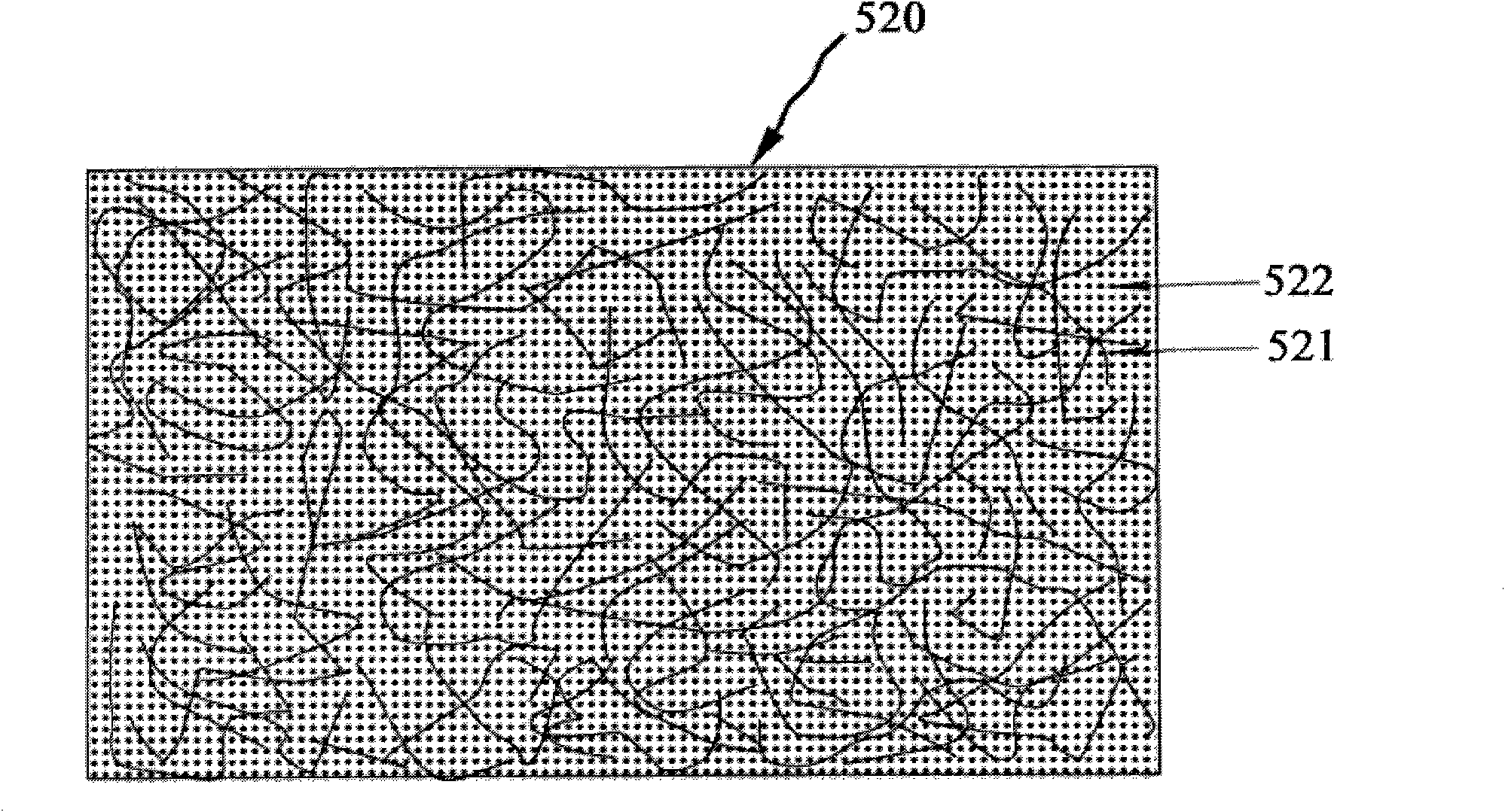
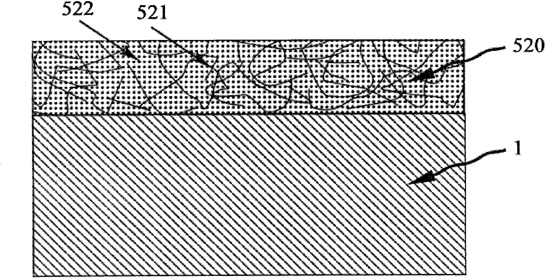
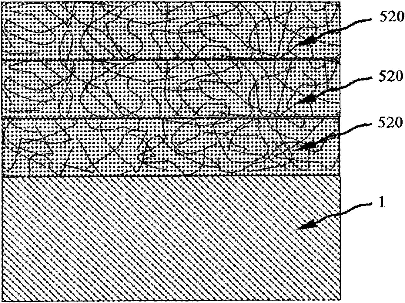
[0063] The guiding ideology of the present invention is in the carbon nanotube-amorphous silicon composite film structure, utilizes carbon nanotube and amorphous silicon respectively excellent electrical and optical property, prepares the composite thin film (as shown in Fig. figure 1 shown), used as infrared light absorption and thermistor materials for microbolometers (such as Figure 5 and 6 shown) to improve device performance. Preparation of carbon nanotube-amorphous silicon composite film embodiment of the present invention is as follows: 1. select silicon wafer as the substrate 1 of thin film growth, first use Piranha solution treatment and deionized water cleaning, then use dilute hydrofluoric acid solution After soaking a...


PUM

PropertyMeasurementUnit
diameteraaaaaaaaaa
lengthaaaaaaaaaa
thicknessaaaaaaaaaa

Abstract

The invention relates to a microbolometer, which comprises a microbridge structure, wherein a thermosensitive resistance material and an infrared absorption material layer in the microbridge structure are of a carbon nanometer tube-amorphous silicon composite film, the carbon nano tube-amorphous silicon composite film is formed by compounding an one-dimension carbon nano-tube and a two-dimensional amorphous silicon film, and the microbridge structure is of a three-layer sandwich structure; the most bottom layer is of a amorphous silicon nitride film which is used as a supporting and insulation material of the microbridge; the intermediate layer is of one layer or multiple layers of carbon nano-tube-amorphous composite film, the stress is opposite to the nature of the bottom layer silicon nitride film, and the carbon nano-tube-amorphous composite film is used as the thermosensitive layer and the infrared absorption layer of the microbolometer; and the surface layer is of an amorphous silicon nitride film, the stress of the amorphous silicon nitride film is opposite to the nature of the intermediate carbon nano-tube-amorphous composite film, and the amorphous silicon nitride film is used as a passivation layer of the inforared sensing film and a control layer of the stress. The microbolometer and the preparation method can overcome the weaknesses of the prior art, improves the working performance of the part, reduces the cost of the raw material and are applicable to the industrialized mass production.

Description

technical field [0001] The invention relates to the technical field of uncooled infrared detection, in particular to a microbolometer and a preparation method thereof. Background technique [0002] Infrared detectors convert invisible infrared heat radiation into detectable electrical signals to realize the observation of external affairs. Infrared detectors are divided into two categories: quantum detectors and thermal detectors. Thermal detectors, also known as uncooled infrared detectors, can work at room temperature, have the advantages of good stability, high integration, and low price, and have broad application prospects in military, commercial, and civilian fields. Uncooled infrared detectors mainly include three types: pyroelectric, thermocouple, and thermistor. Among them, the microbolometer (Microbolometer) focal plane detector based on thermistor has developed very rapidly in recent years. Uncooled infrared detector (see Leonard P. Chen, "Advanced FPAs for Mult...

Claims


Application Information

Patent Timeline
Patent Type & Authority Applications(China)
IPC IPC(8): B81B7/02B81C1/00B82B3/00G01J5/20
Inventor 许向东蒋亚东周东杨书兵王志王晓梅
Owner UNIV OF ELECTRONICS SCI & TECH OF CHINA
Why Eureka
Try Eureka