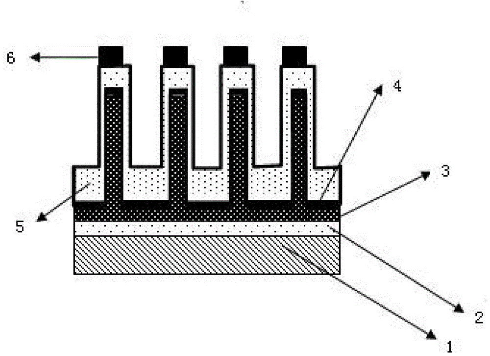
A kind of czts nanoarray thin film solar photovoltaic cell and preparation method thereof
A thin-film solar and photovoltaic cell technology, applied in photovoltaic power generation, circuits, electrical components, etc., can solve the problems of limiting the large-area preparation of nanowire arrays, nanowire impurities, and low production costs, and achieve convenient large-area application and uniform distribution. , the effect of low cost
- Summary
- Abstract
- Description
- Claims
- Application Information
AI Technical Summary
Problems solved by technology
Method used
Image
Examples
Embodiment 1
[0042] The preparation method of the CZTS nano-array thin-film solar photovoltaic cell of the present embodiment comprises the following steps:
[0043] (1) Polish the copper sheet with No. 0-6 sandpaper, and ultrasonically clean it with alcohol, acetone, and deionized water for 5 minutes; then deposit a layer of Mo on the copper sheet by magnetron sputtering, and the thickness of the Mo layer is 50 μm; A layer of zinc film with a thickness of 1 μm is sputtered on the copper sheet deposited with the Mo layer;
[0044] (2) The product of step (1) is mixed with hydrogen sulfide / oxygen mixed gas, wherein the volume percentage of hydrogen sulfide is 1%, and heated at 50°C for 16h to convert the zinc film into a zinc sulfide nanowire array; The final product is used as the working electrode, the platinum wire is used as the counter electrode, the saturated calomel electrode is used as the reference electrode, the acidic solution containing copper chloride is used as the electrolyte...
Embodiment 2
[0050] The preparation method of the CZTS nano-array thin-film solar photovoltaic cell of the present embodiment comprises the following steps:
[0051] (1) The silicon wafer is ultrasonically cleaned with 1mol / L NaOH, 1mol / L HCl solution, absolute ethanol, and deionized water in sequence; then a layer of Au is magnetron sputtered on the silicon wafer, and the thickness of the Au layer is 800nm ; A zinc film with a thickness of 1 μm was sputtered on a silicon wafer deposited with an Au layer;
[0052] (2) The product of step (1) is mixed with hydrogen sulfide / oxygen mixed gas, wherein the volume percentage of hydrogen sulfide is 30%, and heated at 60°C for 500h to convert the zinc film into a zinc sulfide nanowire array; The final product is used as the working electrode, the platinum wire is used as the counter electrode, the saturated calomel electrode is used as the reference electrode, the acidic solution containing copper chloride, tin chloride and selenous acid is used a...
Embodiment 3
[0058] The preparation method of the CZTS nano-array thin-film solar photovoltaic cell of the present embodiment comprises the following steps:
[0059] (1) Electron beam evaporates one deck ITO on the newly cut mica sheet, and the thickness of the ITO layer is 800nm; Evaporate a layer of thickness on the mica sheet after the electron beam evaporates ITO and be the zinc film of 1 μm;
[0060] (2) The product of step (1) is mixed with hydrogen sulfide / oxygen mixed gas, wherein the volume percentage of hydrogen sulfide is 50%, and heated at 60° C. for 12 hours to convert the zinc film into a zinc sulfide nanowire array; The final product is used as the working electrode, the platinum wire is used as the counter electrode, the saturated calomel electrode is used as the reference electrode, the acidic solution containing copper chloride, tin chloride and selenous acid is used as the electrolyte, and sunlight is placed on the outside of the electrolytic cell. The simulator was used...
PUM
| Property | Measurement | Unit |
|---|---|---|
| thickness | aaaaa | aaaaa |
| thickness | aaaaa | aaaaa |
| thickness | aaaaa | aaaaa |
Abstract
Description
Claims
Application Information
