Microcrystalline nickel-phosphorus alloy chemical plating solution and preparation method thereof
A technology of nickel-phosphorus alloy and chemical plating solution, which is applied in the field of information materials, can solve the problems of chip stability and reliability, small contact between nickel-plated layer and silicon layer, adverse effects of subsequent welding, etc., and achieve silicon-based bonding force Good, flat deposition, and the effect of reducing the surface energy of the chip
- Summary
- Abstract
- Description
- Claims
- Application Information
AI Technical Summary
Problems solved by technology
Method used
Image

Examples
Embodiment 1
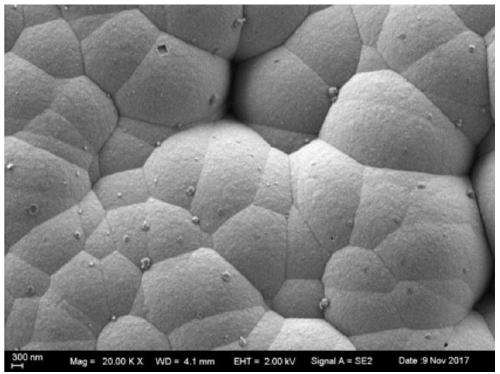
[0036] 120 parts of nickel chloride, 100 parts of ammonium chloride, 200 parts of citric acid, 30 grams of EDTA disodium salt, 50 parts of ammonia water, 30 parts of sodium hypophosphite, dissolved in deionized water, and then added low-foaming fluorocarbon surface active 0.05 part, 1 part of potassium iodide stabilizer, 0.05 part of thiourea, add deionized water to make 4 liters, and ultrafine filter to make working solution. Take 60 pieces of 3-inch monocrystalline silicon wafers and put them on the support (floor) of polytetrafluoroethylene, after activation and hydrolysis, put them into the electroless nickel plating working solution, the temperature is controlled at 85±5°C, and the nickel plating time is 100 seconds . After testing, the thickness of the coating is 0.70μm, the bonding force between the 1A chip and the pad is 38.0N, the coating is microcrystalline, and the number of holes per unit area on both sides of the chip is 0.5 / cm 2 .
[0037] figure 1 and figur...
Embodiment 2
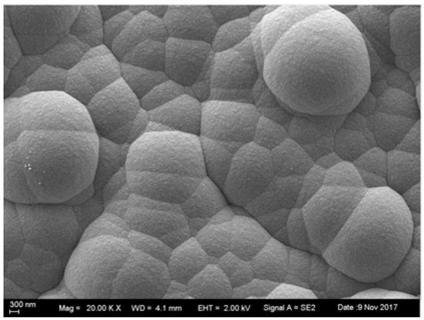
[0039] 60 parts of nickel sulfate, 80 parts of ammonium chloride, 90 parts of ammonium hydrogen citrate, 70 parts of ammonia water, 100 parts of sodium hypophosphite, dissolved in deionized water, then added 3 parts of alkyl diphenyl ether sulfonate, stable Add 0.05 parts of thiourea, 1 part of succinic acid, add deionized water to make 4 liters, and filter it into a working solution; take 60 3-inch single-crystal silicon wafers and put them on the support (floor) of polytetrafluoroethylene , after activation and hydrolysis, put it into the electroless nickel plating working solution, the temperature is controlled at 85±5°C, and the nickel plating time is 100 seconds. After testing, the thickness of the coating is 0.43μm, the bonding force between the 1A chip and the pad is 35.0N, the coating is microcrystalline, and the number of holes per unit area on both sides of the chip is 0.6 / cm 2 .
[0040] image 3 and Figure 4 These are the SEM photos of the boron and phosphorus ...
Embodiment 3
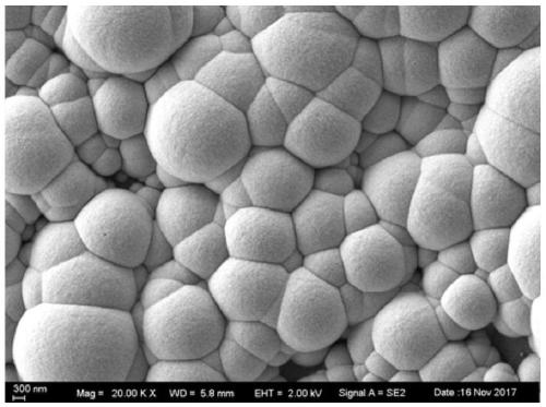
[0042]100 parts of nickel sulfamate, 120 parts of ammonium chloride, 250 parts of triammonium citrate, 30 parts of ammonia water, 70 parts of sodium hypophosphite, dissolved in deionized water, and then added polyoxypropylene-polyoxyethylene block polyether 2 part, 0.04 part of stabilizer benzotriazole, add deionized water to make 4 liters, ultra-micro-filtered into working solution; get 60 3-inch monocrystalline silicon wafers and put them on the support (floor) of polytetrafluoroethylene , after activation and hydrolysis, put it into the electroless nickel plating working solution, the temperature is controlled at 85±5°C, and the nickel plating time is 100 seconds. After testing, the thickness of the coating is 1.12 μm, the bonding force between the 1A chip and the pad is 46N, the coating is microcrystalline, and the number of holes per unit area on both sides of the chip is 0.4 pcs / cm 2 .
PUM
| Property | Measurement | Unit |
|---|---|---|
| Thickness | aaaaa | aaaaa |
| Thickness | aaaaa | aaaaa |
| Thickness | aaaaa | aaaaa |
Abstract
Description
Claims
Application Information
 - R&D
- Intellectual Property
- Life Sciences
- Materials
- Tech Scout
- Unparalleled Data Quality
- Higher Quality Content
- 60% Fewer Hallucinations
Browse by: Latest US Patents, China's latest patents, Technical Efficacy Thesaurus, Application Domain, Technology Topic, Popular Technical Reports.
© 2025 PatSnap. All rights reserved.Legal|Privacy policy|Modern Slavery Act Transparency Statement|Sitemap|About US| Contact US: help@patsnap.com