Method for large-area transfer of two-dimensional transition metal chalcogenide film and application thereof

A technology of chalcogenides and transition metals, which is applied in the field of large-area transfer of two-dimensional transition metal chalcogenides thin films, can solve the problems of easy damage and interface residues, and achieve the effects of reducing residues, reducing interface states, and low cost

Inactive Publication Date: 2020-01-03
NANJING UNIV
View PDF11 Cites 7 Cited by
  • Summary
  • Abstract
  • Description
  • Claims
  • Application Information

AI Technical Summary

Problems solved by technology

[0005] Purpose of the invention: In view of the problems of easy damage and interface residues in the transfer of transition metal chalcogenide thin films in the prior art, the present invention provides a method for large-are

Method used


Image

  • Method for large-area transfer of two-dimensional transition metal chalcogenide film and application thereof
  • Method for large-area transfer of two-dimensional transition metal chalcogenide film and application thereof
  • Method for large-area transfer of two-dimensional transition metal chalcogenide film and application thereof

Examples


Embodiment 1

[0048] (1) Prepare a large-area molybdenum disulfide film on glass by physical vapor growth. The growth conditions are: use molybdenum disulfide powder as the source, place glass as the growth substrate in a tube furnace, and vacuum the tube furnace Finally, 30 sccm of argon gas is introduced as the carrier gas, and the temperature of the furnace body is heated to 900°C, so that the molybdenum disulfide powder evaporates and deposits crystals on the glass. After 30 minutes, a large area of ​​molybdenum disulfide can be formed on the glass surface. film;

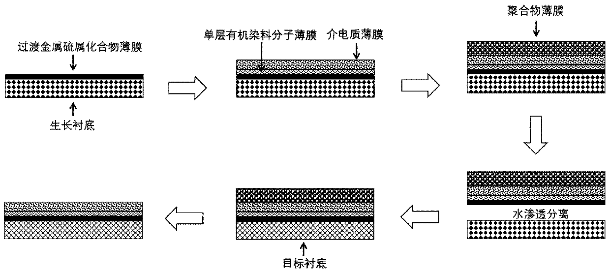
[0049] (2) Using van der Waals epitaxy technology and atomic layer deposition technology to integrate a single layer of 3,4,9,10-perylene tetracarbonyl diimide organic dye molecular film-alumina film on the surface of molybdenum disulfide film, and then Its surface is drop-coated with a layer of polyvinyl alcohol film, and the stacked structure obtained is as follows: figure 2 .

[0050] The growth conditions of monolayer ...

Embodiment 2

[0057] (1) Prepare a large-area molybdenum diselenide film on sapphire by chemical vapor deposition. The growth conditions are: molybdenum oxide powder and selenium powder are used as precursor reactants, and sapphire is used as the growth substrate. , the tube furnace is evacuated thickly, 20sccm argon is introduced as the carrier gas, and the temperature of the furnace body is increased to 800°C, so that the precursor reactants are evaporated and reacted. After one hour of growth, a large area of ​​secondary Molybdenum selenide film;

[0058] (2) Using van der Waals epitaxy technology and atomic layer deposition technology to integrate a single layer of 3,4,9,10-perylenetetraacid dianhydride organic molecular film-alumina film on the surface of molybdenum diselenide film, and then on its surface Spin-coat a layer of polymethyl methacrylate film to obtain polymethyl methacrylate film / alumina film-single-layer 3,4,9,10-perylenetetraacid dianhydride molecular film / molybdenum di...

Embodiment 3

[0066] (1) Prepare a large-area molybdenum disulfide film on silicon oxide by chemical vapor deposition. The growth conditions are: use molybdenum oxide powder and sulfur powder as reaction precursors, use silicon oxide as the growth substrate, and place them in a tube furnace at intervals In the process, the tube furnace is evacuated thickly, 100sccm argon is introduced as the carrier gas, and the temperature of the furnace body is heated to 700°C, so that the molybdenum disulfide powder evaporates and deposits crystals on the silicon oxide. After 10 minutes, it can be in A large area of ​​molybdenum disulfide film is formed on the surface of silicon oxide.

[0067] (2) Using van der Waals epitaxy technology and atomic layer deposition technology to integrate a single 3,4,9,10-perylene tetracarbonyl diimide organic molecular film-hafnium oxide film on the surface of the molybdenum disulfide film, and then on the surface A layer of polystyrene film is scraped and coated to obt...


PUM

PropertyMeasurementUnit
Thicknessaaaaaaaaaa

Abstract

The invention discloses a method for large-area transfer of a two-dimensional transition metal chalcogenide film and an application thereof. The method comprises the following steps: preparing a large-area two-dimensional transition metal chalcogenide film; sequentially depositing a single-layer organic dye molecular film and a dielectric film on the surface of the transition metal chalcogenide film by adopting a Van der Waals epitaxial growth technology and an atomic layer deposition technology, and arranging a layer of polymer film; and carrying out separation to obtain a transition metal chalcogenide/single-layer organic dye molecule/dielectric/polymer composite film based on a water permeation separation principle, combining the composite film with a target substrate, and removing thepolymer film to finish transfer. The transferred two-dimensional transition metal chalcogenide film has large-area integrity and a pollution-free interface. The transferred two-dimensional transitionmetal chalcogenide/single-layer organic dye molecular film-dielectric film can be used as a channel layer and a dielectric layer of an electronic device, has extremely low electric leakage and interface state, and can reduce the working voltage of the electronic device.

Description

technical field [0001] The invention relates to a large-area transfer method of a two-dimensional transition metal chalcogen compound thin film and its application in the preparation of electronic or optoelectronic devices, belonging to the technical field of two-dimensional material electronic devices. Background technique [0002] Since Gordon Moore proposed Moore's Law, the number of devices integrated on an integrated circuit chip has doubled every 18 months, and the performance of microprocessors has doubled every 18 months; at the same time, the size of transistors is also shrinking. Currently, commercial chips have been developed to the 10nm node. However, as the scale approaches the quantum limit, the leakage and power consumption problems caused by the short-channel effect restrict the continuous shrinking process of transistors. Researching new two-dimensional materials is one of the important ways to continue Moore's Law. Transition metal chalcogenides are a cl...

Claims


Application Information

Patent Timeline
IPC IPC(8): H01L21/34H01L21/683H01L21/44H01L29/24H01L29/423H01L29/49H01L29/51H01L29/786C23C14/06C23C14/12C23C14/24C23C16/30C23C16/40C23C16/455
CPCH01L29/66969H01L29/78603H01L29/78696H01L29/78609H01L29/24H01L29/401H01L29/42364H01L29/4908H01L29/517H01L21/6835C23C14/24C23C14/0623C23C14/12C23C16/45525C23C16/403C23C16/405C23C16/305H01L2221/68381
Inventor 王欣然李卫胜施毅
Owner NANJING UNIV
Why Eureka
Try Eureka