[0026] The present invention provides microdischarge devices and arrays of microdischarge devices that are inexpensive to manufacture and have electrical and optical characteristics that are superior to previous microdischarge devices. These microdischarge devices and arrays may operate at
atmospheric pressure and at voltages of 120V or less, and preferably at voltages of not greater than 100 V. Either
direct current (DC) or
alternating current (AC) voltages may be applied to the electrodes. The microdischarge devices and arrays of microdischarge devices may also be flexible.
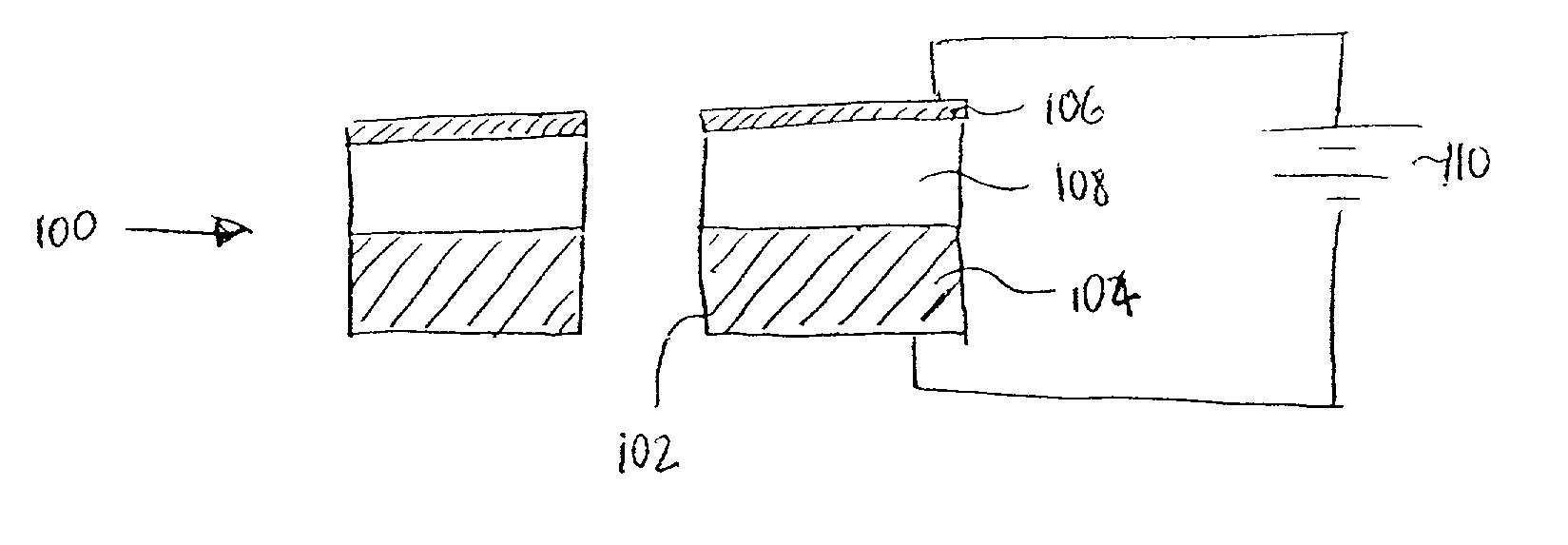
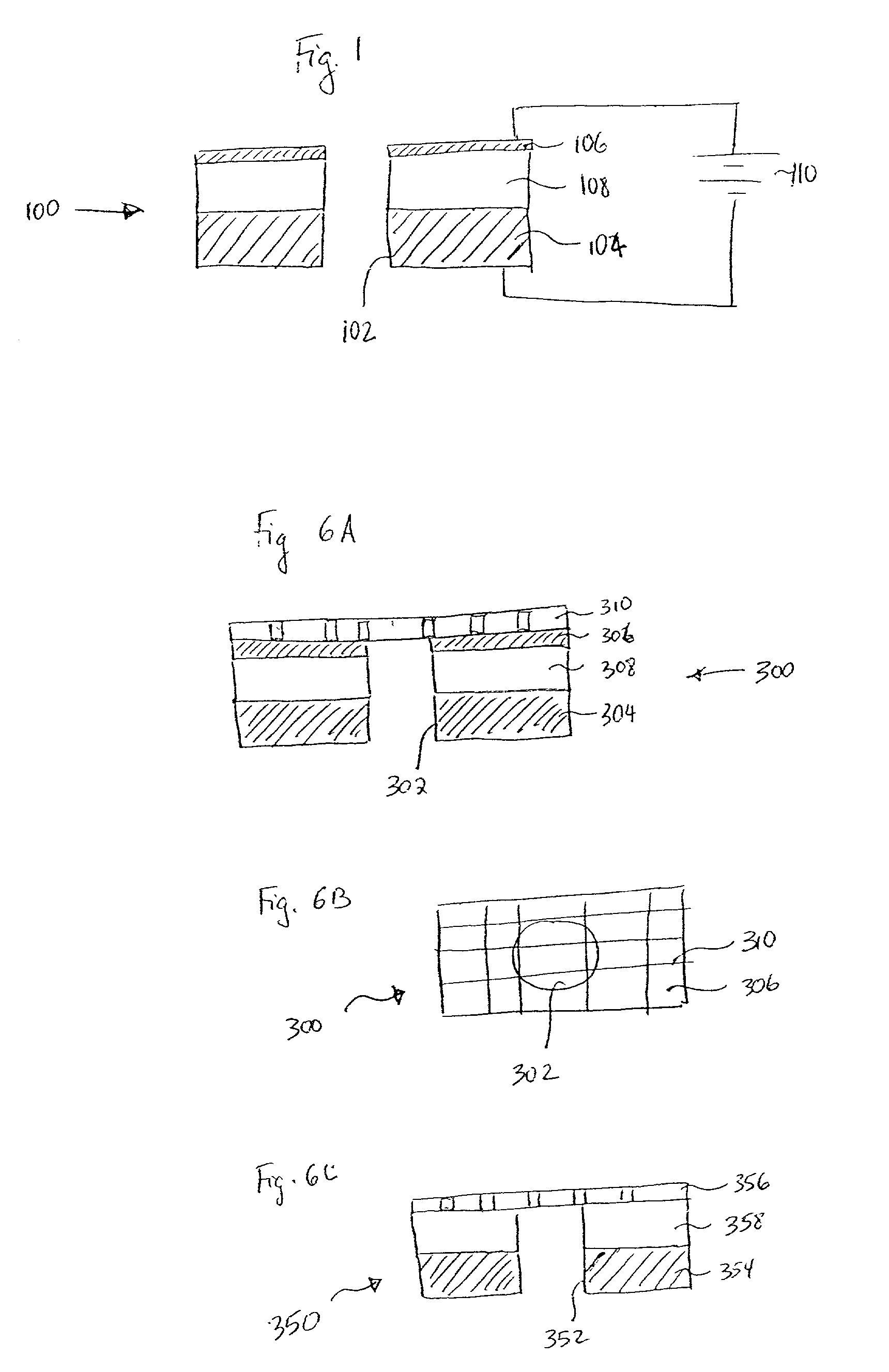
[0027] An embodiment of a microdischarge device (not drawn to scale) is shown in FIG. 1. The microdischarge device 100 includes a first
electrode 106, a second
electrode 104 and a
dielectric layer 108 (also called an insulating layer or an insulator) disposed between the first
electrode 106 and second electrode 104. A cavity 102 is formed in the insulator 108 and may be additionally formed in either or both of the first electrode 106 and the second electrode 104 such that the openings or holes in each of the first electrode 106, insulator 108, and second electrode 104 are aligned with each other. The cavity 102 preferably has a substantially cylindrical shape to more easily couple to
optical fiber, for example, and is formed in a direction transverse to the planes containing the electrodes 104 and 106 and insulator 108. The first electrode 106 and second electrode 104 are both electrically and thermally conductive and a
potential difference across the insulator 108 is established by a
voltage source 110 connected between the first electrode 106 and the second electrode 104. The
potential difference creates a
discharge in the cavity 102 when a gas is present. The resulting light has emission spectra that are characteristic of the gas selected. This light is subsequently emitted from at least one end of the cavity 102.
[0028] The first electrode 106 and second electrode 104 preferably serve to establish the
potential difference across the insulator 108 and thereby energize the microdischarge device 100. Thus, the first electrode 106 and second electrode 104 are fabricated from materials having good electrical and
thermal conductivity. The first electrode 106 and second electrode 104 may be planar and may be fabricated from thin
layers of conductive material, preferably having a thickness of less than 100 .mu.m, more preferably thicknesses from about 10 .ANG.-10 .mu.m and from 50 .ANG.-5 .mu.m. Common metals that may be used to form the electrodes include
copper, aluminum, gold, silver,
nickel, and
zinc and alloys thereof. Other conductors include polymers containing
carbon black and other conducting
polymer materials or highly doped crystalline, polycrystalline or amorphous
semiconductor films. Alternatively, rather than the electrodes being formed from an optically opaque material, at least one of the electrodes may be fabricated from a
solid layer of optically transmissive material that does not significantly absorb light at the
wavelength of the discharge, such as
indium tin oxide (ITO). Optically transmissive material transmits preferably at least 50% of the light impinging substantially normal to the surface of the material at
wavelength emitted by the discharge. More preferably, the optically transmissive material transmits at least 60%, 70%, 80%, 90%, or even 95% of the light impinging substantially normal to the surface of the material at a
wavelength emitted by the discharge. The first electrode 106 and second conducting electrode 13 preferably form a cathode and an anode.
[0033] The insulator 108 may be a
polymer such as
polyimide, which has exceptional
thermostability and
dielectric strength. For example, the
breakdown voltage for a
polyimide film about 5 .mu.m thick is approximately 1.2 kV, giving a
dielectric strength in excess of 10.sup.6 V-cm. Other dielectrics, resins and polymers--for example,
oxide and
nitride films such as
metal oxides, SiO.sub.2, Si.sub.3N.sub.4 or
KAPTON--may be used as long as the material retains its insulation properties at the material thickness required for adequate
dielectric strength. Furthermore, multiple films of different materials (having different dielectric constants) may be used to fabricate the insulator in order to improve both individual device and
array performance. Tests have shown that a
multiple layer dielectric (containing, for example, .about.0.5 .mu.m Si.sub.3N.sub.4, 0.5 .mu.m SiO.sub.2, and several microns of
polyimide) not only improves the
voltage-current characteristics of an individual microdischarge device but also makes it possible to realize stable operation of large arrays (for example, 30.times.30) of devices. If, on the other hand, the insulator 108 is a single film of polyimide, for example, it is difficult to operate arrays larger than approximately 5.times.5.
[0037] The microdischarge device 100 may be less than 50 .mu.m thick (approximately two one-thousandths of an inch), thus giving rise to a thinner device than is typical of conventional microdischarge devices. One feature of arrays of such devices is that the finished array may be flexible and light. Thus, these arrays are able to conform to various shapes and can, if desired, be rolled into a tube. This feature enhances the portability and utility of microdischarge arrays.
[0045] Sealing of the microdischarge cavity while containing the desired gas at the proper pressure may be performed in a number of ways other. One method is to "hard seal" the array of microdischarge electrodes and insulator to a
quartz window having a conducting film (such as ITO) or a fine
metal grid on one side. The
bonding process takes place with the conductor facing the electrode and bonding occurs along the entire perimeter of the electrode and quartz. When completed, this structure is robust and compact, requiring only electrical connections to an appropriate power supply. Another approach using flexible optically transmissive material is to laminate an array of electrode / insulator / elec-trode (or screen) devices. By laminating a plastic sheet on both sides of the microdischarge array
assembly, light generated within the array will be transmitted by the packaging if the laminating
sheet material is chosen properly. A
phosphor / electroluminescent material may also be included on the screen before sealing.

