Film with transparent electroconductive membrane and its use

a technology of electroconductive membrane and film, which is applied in the direction of conductive layers on insulating supports, instruments, transportation and packaging, etc., can solve the problems of unavoidable step of developing a resist, deformation, and significantly inferior heat resistance or moisture resistance of conventional synthetic resin films, and achieve excellent acid resistance, good surface flatness, and high luminescence brightness

Inactive Publication Date: 2009-11-26
DAI NIPPON PRINTING CO LTD
View PDF9 Cites 20 Cited by
  • Summary
  • Abstract
  • Description
  • Claims
  • Application Information

AI Technical Summary

Benefits of technology

[0041]The film with a transparent electroconductive membrane according to the first invention comprises a transparent base material and a transparent electroconductive membrane, the transparent electroconductive membrane having on its surface crystalline secondary particles having an average particle diameter of 0.1 to 1 μm in an amount of 1 to 100 particles/μm2. By virtue of the above constitution, the film with a transparent electroconductive membrane according to the first invention can provide a display having a good surface flatness and a high luminescence brightness, and a substrate for a display, a display, a liquid crystal display device, and an organic EL element using the film with a transparent electroconductive membrane.
[0042]The film with a transparent electroconductive membrane according to the first invention has excellent acid resistance.
[0043]The film with a transparent electroconductive membrane according to the second invention comprises a transparent base material and a transpa...

Problems solved by technology

Conventional synthetic resin films, however, are significantly inferior in heat resistance or moisture resistance to glass substrates.
Accordingly, deformation, for example, upon heating in the step of forming a thin metal film by vapor deposition or the like, or upon heating in the step of curing by heating after coating of a heat curable resin coating material, or deformation caused by moisture absorption upon contact with an aqueous solution in the step of etching a thin metal film or the step of developing a resist is unavoidable.
Consequently, problems occur such as a deterioration in flatness of the formed display or ...

Method used


Image

  • Film with transparent electroconductive membrane and its use
  • Film with transparent electroconductive membrane and its use
  • Film with transparent electroconductive membrane and its use

Examples


example a

[0213]The first invention is further illustrated by the following Examples and Comparative Examples that are not intended as a limitation of the invention.

[0214]Materials and formation methods for individual layers used in the Examples and Comparative Examples will be summarized.

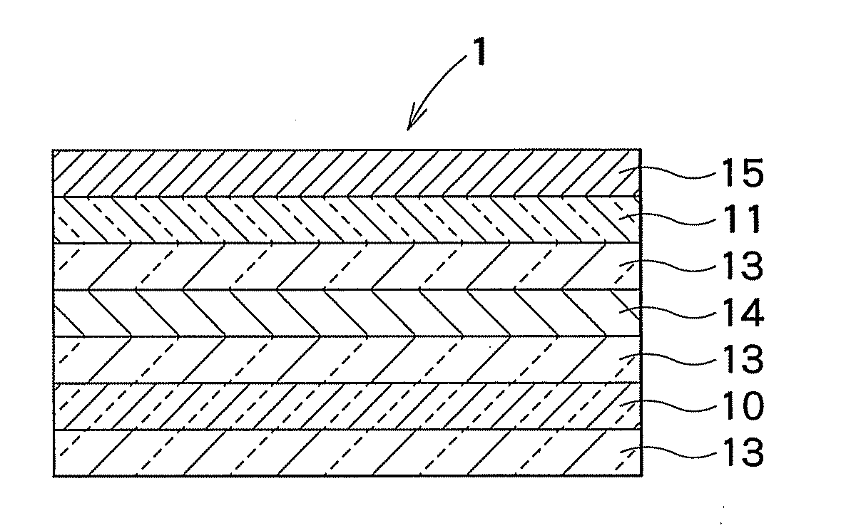
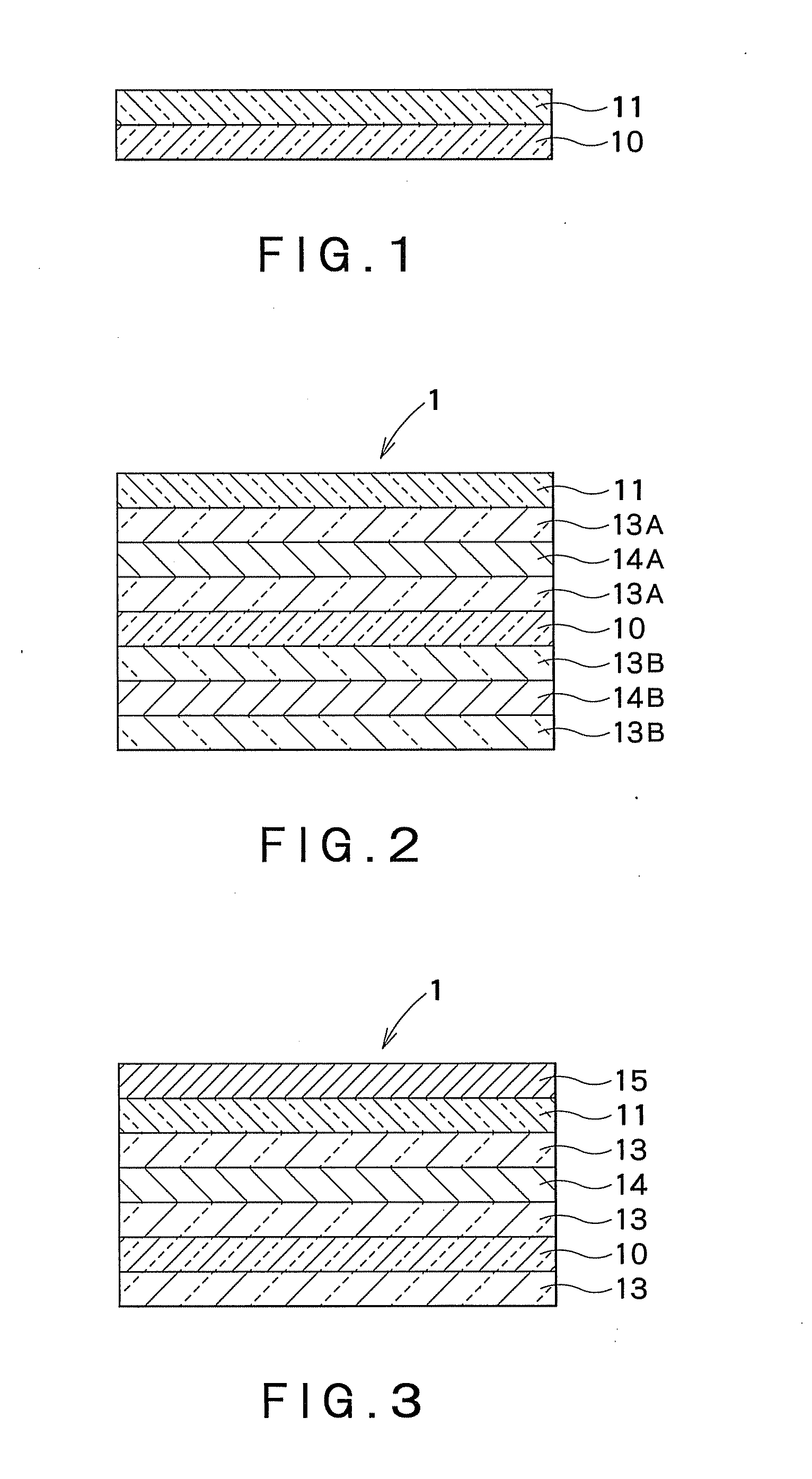
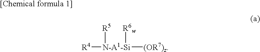
[0215](1) Base Material:

[0216]“Polyethylene naphthalate” (manufactured by Teijin Ltd., Teonex Q65 (100 μm)) was used as a base material in the Examples.

[0217](2) Smoothing Layer:

[0218]A sol-gel layer used as a smoothing layer was formed by spin coating a coating agent composed mainly of an aminoalkyltrialkoxysilane, drying the coating on a hot plate at 120° C. for two min and then in an oven at 160° C. for one hr to form a 1.2 μm-thick sol-gel layer (a flattening layer).

[0219]An UV cured resin layer used as a smoothing layer was formed by coating the following UV cured resin composition, drying the coating at 120° C. for two min, and then applying ultraviolet light (UV) with a high pressure mercury lamp to c...

example a1

[0243]A 0.5 nm-thick ITO film was formed on a base material by magnetron sputtering using ITO as a target under conditions of electric power 2.0 kW and Ar gas 500 sccm and was held in vacuum for 15 sec. These two steps were repeated 300 times to form a 150 nm-thick ITO film. For the ITO film as the uppermost layer, the particle diameter of the crystalline secondary particles and the number of crystalline secondary particles were measured and were found to be 0.3 μm and 5 particles / μm2, respectively. The half-width value in the maximum peak of the crystal phase was 4.15. In order to form a 15-μm line by photolithography, the ITO layer was patterned with an etching liquid. As a result, the residue of the ITO particles was not observed under an optical microscope, and good patterning could be realized.

example a2

[0244]A 15 nm-thick ITO film was formed on a base material by a resistance heating-type vacuum deposition method. ITO particles were used as a material for the vapor deposition. The heating temperature was 1500° C. Plasma treatment was then carried out using a DC power supply under conditions of electric power 1 kW, Ar 200 sccm, and oxygen 500 sccm for 15 sec. These two steps were repeated ten times to form a 150 nm-thick ITO film. For the ITO film as the uppermost layer, the particle diameter of the crystalline secondary particles and the number of crystalline secondary particles were measured and were found to be 0.8 μm and 15 particles / μm2, respectively. The half-width value in the maximum peak of the crystal phase was 6.50. In order to form a 15-1 μm line by photolithography, the ITO layer was patterned with an etching liquid. As a result, the residue of the ITO particles was not observed under an optical microscope, and good patterning could be realized.


PUM

PropertyMeasurementUnit
Lengthaaaaaaaaaa
Transparencyaaaaaaaaaa
Nanoscale particle sizeaaaaaaaaaa

Abstract

This invention provides a film with a transparent electroconductive membrane, which can provide a display having a good surface flatness and possessing a high luminescence brightness, and a substrate for a display, a display, a liquid crystal display device, and an organic EL element using the film with a transparent electroconductive membrane. More specifically, this invention provides a film with a transparent electroconductive membrane, comprising a transparent base material and a transparent electroconductive membrane, the transparent electroconductive membrane having on its surface crystalline secondary particles having an average particle diameter of 0.1 to 1 μm in an amount of 1 to 100 particles/μm2, and a substrate for a display, a display, a liquid crystal display device, and an organic EL element using the film with a transparent electroconductive membrane.

Description

TECHNICAL FIELD[0001]The present invention relates to a film with a transparent electroconductive membrane. More specifically, the present invention relates to a highly transparent film with a transparent electroconductive membrane, which has a high total light transmittance and has suppressed coloring, a substrate for a display comprising the film with a transparent electroconductive membrane, a display, a liquid crystal display device, and an organic EL element.BACKGROUND ART[0002]Various display-type displays have hitherto been used, and studies have been made on practice use of these displays. All the displays except for cathode ray tube types aim at thinning, and flexible displays have also become desired.[0003]These have led to studies on the use of synthetic resin sheets or films instead of glass substrates which have hitherto constituted displays. Further, studies have also been made on substrates for displays using gas barrier films for cutting off oxygen and water vapor fr...

Claims


Application Information

Patent Timeline
IPC IPC(8): B32B5/16
CPCG02F1/133305G02F1/1334G02F1/13439H01L51/0097H01L51/5237Y10T428/25Y02E10/549H01B5/14H01B13/0026Y10T428/24372Y10T428/1095H01L2251/305C09K2323/061H10K77/111H10K50/81H10K2102/101H10K50/844
Inventor SAKAKURA, OSAMU
Owner DAI NIPPON PRINTING CO LTD
Why Eureka
Try Eureka