Silicon Nanoparticle Embedded Insulating Film Photodetector

a silicon nanoparticle and photodetector technology, applied in the field of photodetectors, can solve the problems of inefficient materials for optoelectronic devices, inability to provide the wide range of optical dispersion characteristics required, and inability to achieve the wide range of optical dispersion characteristics of single thin film material, etc., to achieve high photocurrent, low capacitance, and high sensitivity-bandwidth product

Inactive Publication Date: 2009-12-03
SHARP LAB OF AMERICA INC
View PDF7 Cites 7 Cited by
  • Summary
  • Abstract
  • Description
  • Claims
  • Application Information

AI Technical Summary

Benefits of technology

[0014]The present invention describes a photodetector made from semiconductor nanoparticles (e.g., nc-Si) embedded Si insulating films, such as SiOxNy thin films. The nc-semiconductor particles embedded in the insulating matrix generate high photo-current at low reverse biases. The high SNR of the nc-semiconductor embedded Si insulating thin films overcome the limitations of conventional Si and wide-band gap semiconductor-based photodetectors. The photoconduction in the nc-semiconductor embedded Si insulating thin films makes possible metal-film-m...

Problems solved by technology

While a single layer device would obviously be more desirable, no single thin-film material has been able to provide the wide range of optical dispersion characteristics required to get the desired optical absorption, band-gap, refractive index, reflection, or transmission over a wide optical range extending from ultraviolet (UV) to far infrared (IR) frequencies.
However, the indirect band-gap makes it an inefficient material for optoelectronic devices.
Si is an indirect bandgap semiconductor with limited speed-responsivity performance, but it is still useful for detection in UV-VIS (visible)-NIR (near-IR) spectrum.
However, the indirect bandgap of Si limits the critical wavelength of Si to 1.12 μm, beyond which its absorption goes to zero, making it insensitive to two primary telecommunication wavelengths of 1.30 and 1.55 μm.
An additional issue with Si based photo-detectors is the dark current limiting the signal-to-noise ratio (SNR), and the thermal instability at operating temperatures higher than 50° C.
However, conventional PECVD and sputtering techniques have the limitations of low plasma density, inefficient power coupling to the plasma, low ion/neutral ratio, and uncontrolled bu...

Method used


Image

  • Silicon Nanoparticle Embedded Insulating Film Photodetector
  • Silicon Nanoparticle Embedded Insulating Film Photodetector
  • Silicon Nanoparticle Embedded Insulating Film Photodetector

Examples


Embodiment Construction

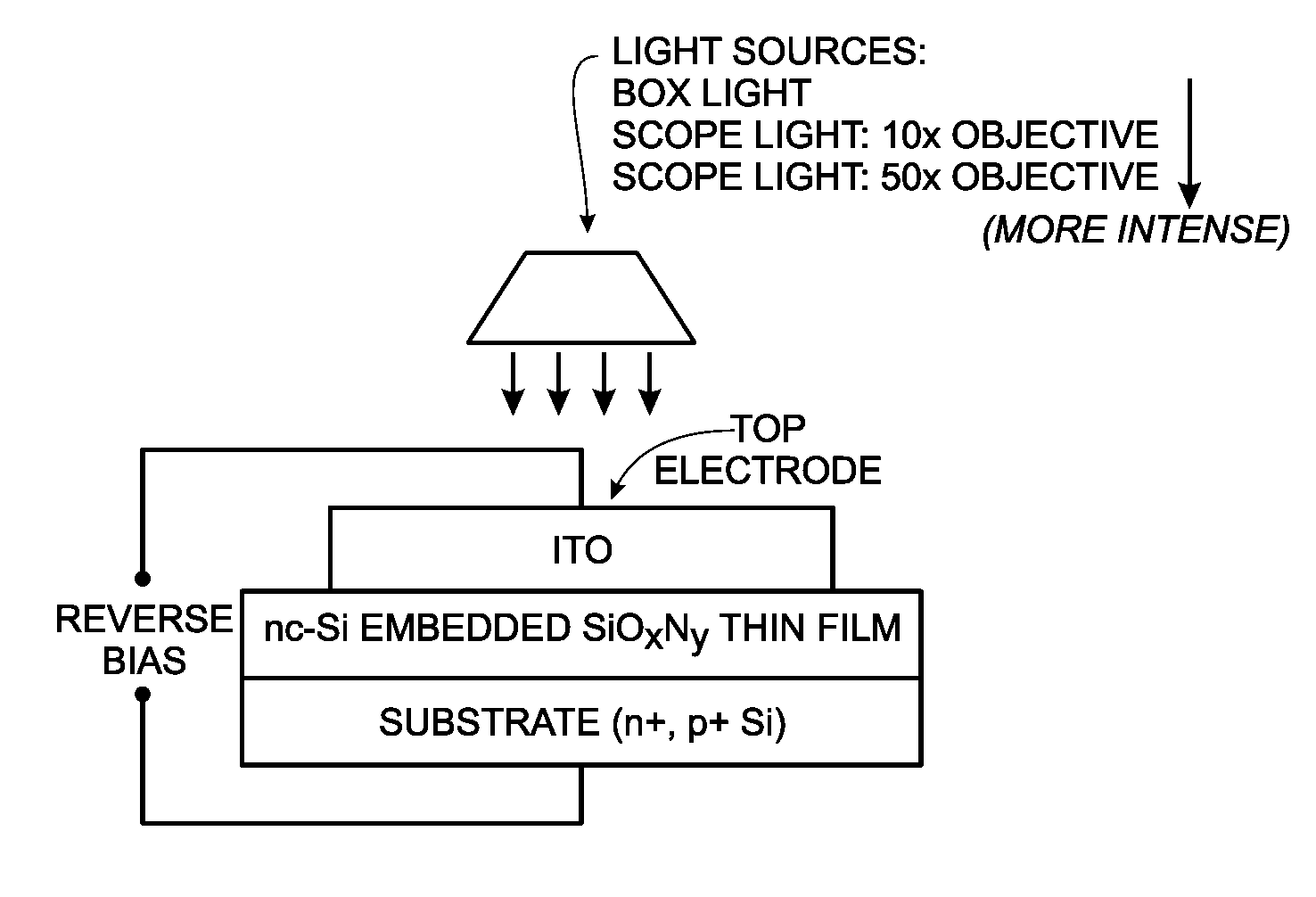
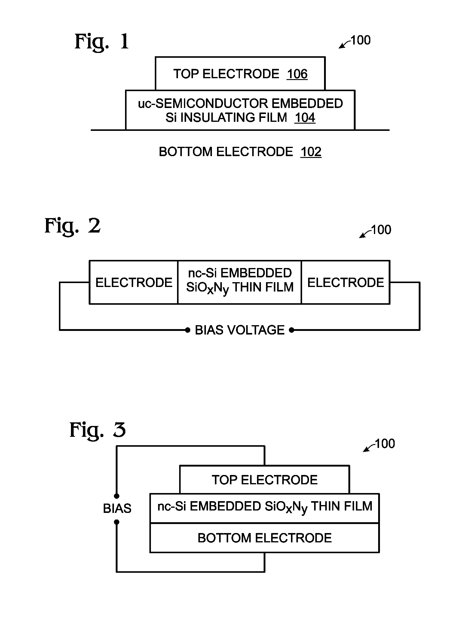
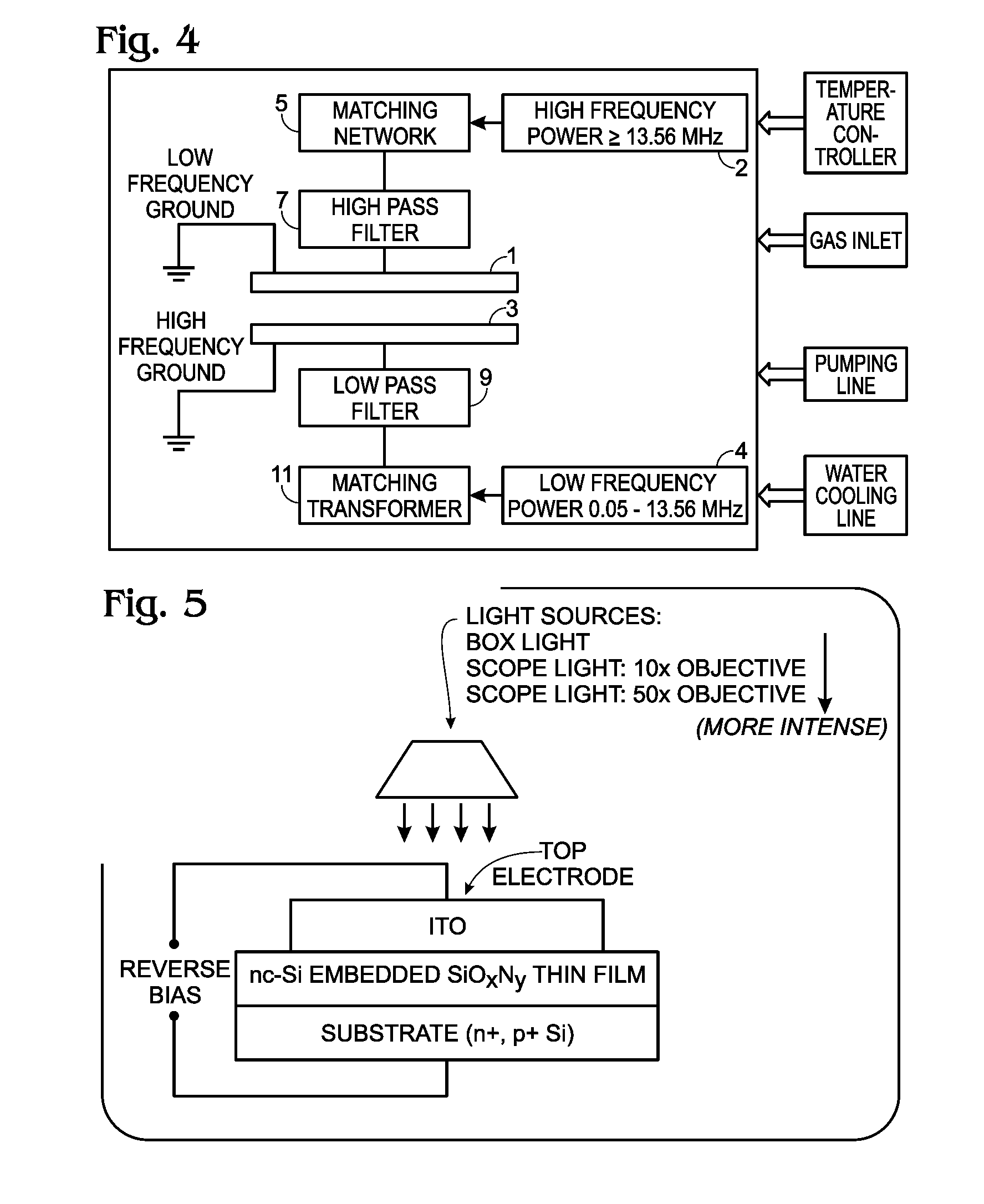
[0030]FIG. 1 is a partial cross-sectional view of a photodetector employing a semiconductor nanoparticle embedded insulating film. The photodetector 100 comprises a bottom electrode 102, which may be a doped semiconductor, metal, or polymer. A semiconductor nanoparticle embedded Si insulating film 104 overlies the bottom electrode 102. The insulating film includes either N or C elements. In one aspect, the Si insulating film 104 is a non-stoichiometric SiOX1NY1 thin-film, where (X1+Y11>0). In another aspect, the Si insulating film 104 is a SiCX thin film, where X<1.

[0031]The semiconductor nanoparticles embedded in the Si insulating film 104 have a diameter in the range of about 1 to 10 nanometers (nm), and are made from either Si or Ge. The semiconductor nanoparticle embedded Si insulating film 104 exhibits a spectral response in a wavelength range of about 200 nanometers (nm) to about 1600 nm. A transparent electrode 106, such an indium tin oxide (ITO) or a thin metal, overlies the...


PUM

PropertyMeasurementUnit
Temperatureaaaaaaaaaa
Diameteraaaaaaaaaa
Lengthaaaaaaaaaa

Abstract

A photodetector is provided with a method for fabricating a semiconductor nanoparticle embedded Si insulating film for photo-detection applications. The method provides a bottom electrode and introduces a semiconductor precursor and hydrogen. A thin-film is deposited overlying the substrate, using a high density (HD) plasma-enhanced chemical vapor deposition (PECVD) process. As a result, a semiconductor nanoparticle embedded Si insulating film is formed, where the Si insulating film includes either N or C elements. For example, the Si insulating film may be a non-stoichiometric SiOXNY thin-film, where (X+Y<2 and Y>0), or SiCX, where X<1. The semiconductor nanoparticles are either Si or Ge. Following the formation of the semiconductor nanoparticle embedded Si insulating film, an annealing process is performed.

Description

BACKGROUND OF THE INVENTION[0001]1. Field of the Invention[0002]This invention generally relates to the fabrication of integrated circuit (IC) photodetectors, and more particularly, to a photodetector made from a silicon (Si) nanoparticle embedded insulating film, using a high-density plasma-enhanced chemical vapor deposition process.[0003]2. Description of the Related Art[0004]The fabrication of integrated optical devices involves the deposition of materials with suitable optical characteristics such as absorption, transmission, and spectral response. Thin-film fabrication techniques can produce diverse optical thin films, which are suitable for the production of large area devices at high throughput and yield. Some optical parameters of importance include refractive index and the optical band-gap, which dictate the transmission and reflection characteristics of the thin film.[0005]Typically, bilayer or multilayer stack thin-films are required for the fabrication of optical devices...

Claims


Application Information

Patent Timeline
IPC IPC(8): H01L31/00H01L21/00
CPCC23C16/308C23C16/505Y02E10/547H01L31/1085H01L31/1804H01L31/0352Y02P70/50
Inventor JOSHI, POORAN CHANDRAZHANG, HAOVOUTSAS, APOSTOLOS T.
Owner SHARP LAB OF AMERICA INC
Why Eureka
Try Eureka