[0031]According to the present invention, by laminating a
titanium dioxide layer and a titanate compound layer having
perovskite crystals, a capacitor material can be obtained in which a capacitor having high withstand
voltage and
low leakage current, unable to be obtained with either layer alone, can be obtained. If the thickness of an insulating material is reduced in one layer only, dielectric breakdown occurs or leakage current increases. In contrast, in the present invention, by laminating (arranging electrically in series) a
titanium dioxide having high withstand
voltage and an insulator having
low leakage current, it was found that an insulating material is obtained having high withstand voltage and low leakage current. As shown in FIG. 1, for example, this material (reference symbol 2 indicates the titanate compound layer having
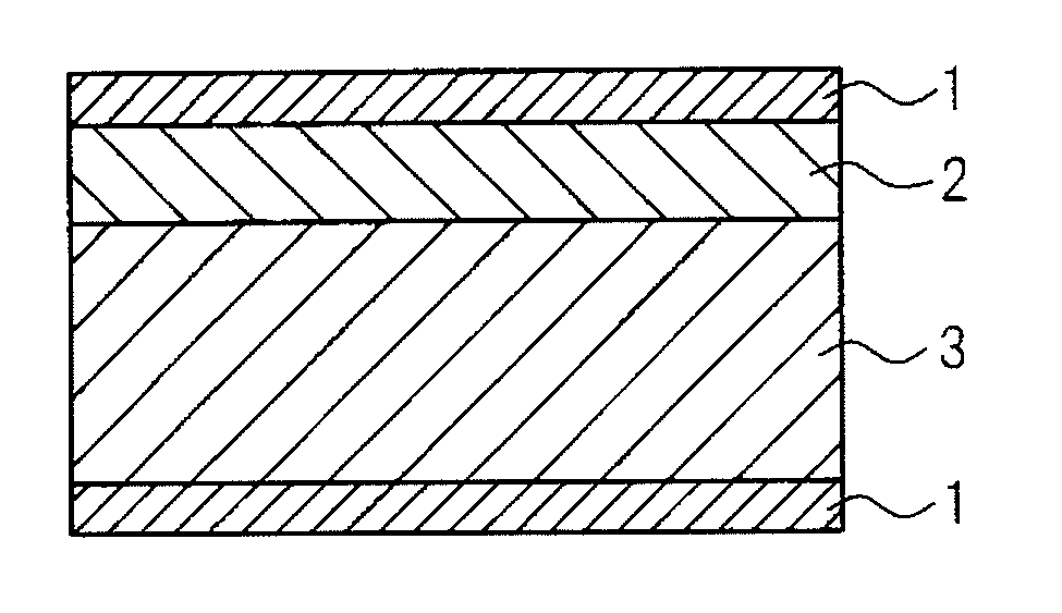
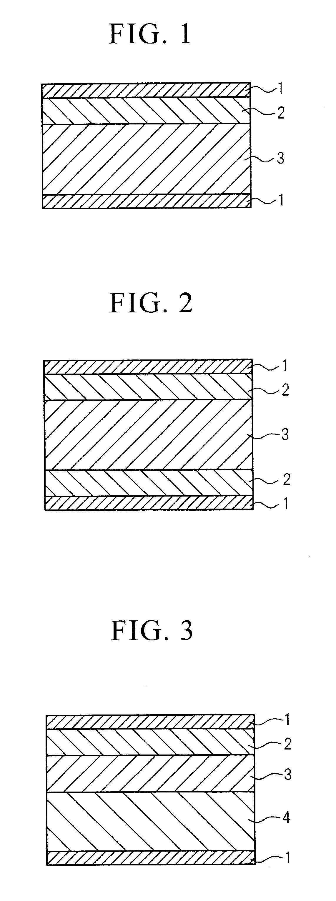
perovskite crystals, while reference symbol 3 indicates the titanium dioxide layer) can be favorably used as a capacitor by forming electrodes 1 on this material. In addition, as shown in FIG. 2, two or more of the same insulating material
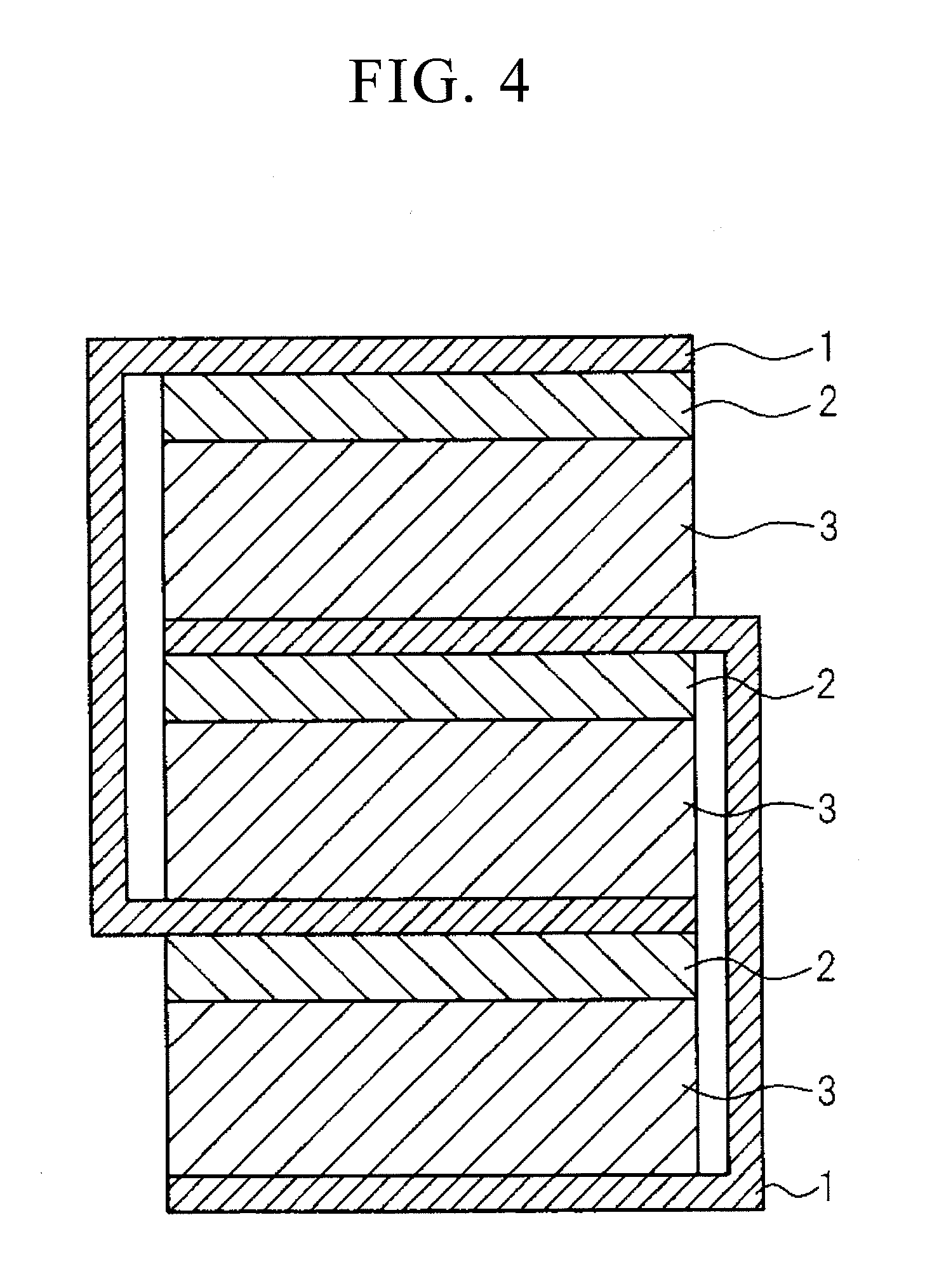
layers can be used, or as shown in FIG. 3, three or more types of insulating materials can be used (reference symbol 4 indicates another insulating layer). In addition, as shown in FIG. 4,
capacitance can be increased by laminating the materials shown in FIGS. 1 to 3 in parallel. It is desirable that the thickness including the electrodes be as thin as possible with respect to compact size and increased functional sophistication of the device, and is preferably set to a thickness of 200 μm or less. A thickness if 100 μm or less is even more preferable since it facilitates formation of a capacitor within a wiring board. Although the voltage at which dielectric breakdown occurs becomes lower then the thickness of the electrical insulating material decreases, the
capacitance of the capacitor increases. Consequently, the thicknesses of various electrical insulating materials are determined based on the desired withstand voltage and
capacitance of the capacitor. In the method of the present invention, a titanium dioxide layer of a prescribed thickness is formed in advance, and
metal ions are reacted with a portion of this titanium dioxide layer. Thus, a titanate compound layer having a perovskite
crystal structure can be formed on the titanium dioxide layer by an extremely easy method. Consequently, a capacitor material can be produced at low cost without requiring the use of complex and elaborate equipment. Desired layer thicknesses can be obtained since there is a correlation between the thickness of the titanium dioxide layer formed in advance and the titanate compound layer obtained following the reaction based on the materials used and the production conditions.
[0032]The formation of these
layers facilitates easier handling if carried out on a substrate. An
electrically conductive material can be used for the substrate, and the substrate can be used directly as an
electrode when forming the capacitor. In addition, an insulating material can be used for the substrate and it may also be used directly as an insulating layer (see, for example, reference symbol 4 in FIG. 3).
[0033]In particular, if
metal titanium or an
alloy containing titanium is used for the substrate and a titanium dioxide layer is formed on the surface thereof by, for example,
anodizing the substrate, the thickness of the titanium dioxide layer can be easily controlled. A titanate compound layer having a perovskite
crystal structure can be formed on the titanium dioxide layer by reacting an
aqueous solution containing at least one type of metal
ion selected from the group consisting of Ca, Sr and Ba with the titanium dioxide layer.
[0034]Here, the use of an alkaline
aqueous solution of pH 11 or higher for the solution containing Ca, Sr or Ba ions enables the formation of a titanate compound layer having a perovskite
crystal structure having few defects, thereby allowing the obtaining of a capacitor having low
dielectric loss tangent. If a basic compound that becomes a gas by at least one means from among
evaporation, sublimation and
thermal decomposition under
atmospheric pressure or reduced pressure is used for the alkaline component of this alkaline solution, decreases in electrical properties of the capacitor caused by alkaline components remaining in the titanate compound layer can be inhibited, thereby allowing the obtaining of a capacitor having stable properties. In addition, the use of
reaction temperature of 80° C. or higher allows the reaction to proceed more reliably. Although a higher
reaction temperature is preferable in terms of the reaction proceeding, if a
hydrothermal reaction occurs in a pressurized container due to reacting at a temperature equal to or higher than the
boiling point of the
aqueous solution, an insulator having a
bilayer structure is not formed, thereby preventing the formation of a titanate compound layer having a perovskite
crystal structure that extends to the interface with the base material.
[0035]A capacitor material obtained in this manner, in which a titanium dioxide layer and a titanate compound layer having a perovskite
crystal structure are laminated, has
high capacitance density. A capacitor produced with this material has a configuration in which a titanium dioxide layer and a titanate compound layer having perovskite crystals are arranged electrically in series between two electrodes. Consequently, in the case of a capacitor having only the two
layers as dielectrics, the capacitance thereof is determined nearly entirely by the titanium dioxide layer having the lower dielectric constant. Consequently, as a result of using a titanate compound layer having a perovskite
crystal structure and high dielectric constant, even if, for example,
barium titanate, which exhibits capacitance properties highly dependent on temperature and current bias voltage, is used, the effects thereof can be suppressed to a low level. In addition,
metal electrodes, for example, can be formed directly without using electrodes in which an
electrolyte,
electrically conductive polymer or other dielectric film can be reoxidized due to low leakage current. As a result, high-frequency properties are improved, and the capacitor obtained in the present invention normally has an electrostatic capacitance at 1 MHz of 80% or more of that at 100 Hz. In addition, reduced material thickness and process simplification can be expected since there is no need to use an
electrolyte, electrically
conductive polymer or carbon paste and the like. Thus, the capacitor obtained in the present invention is preferable for use as a capacitor or other
electronic component, and allows
reduced size of electronic components as well as
reduced size and weight of electronic devices containing these electronic components.

