

Low dielectric constant materials and method
a dielectric constant and low technology, applied in the direction of synthetic resin layered products, transportation and packaging, semiconductor/solid-state device details, etc., can solve the problems of degrading circuit performance, increasing leakage, and affecting the performance of circuits, so as to achieve high mechanical stability, high rotational flexibility, and high thermal stability
- Summary
- Abstract
- Description
- Claims
- Application Information
AI Technical Summary
Benefits of technology
Problems solved by technology
Method used
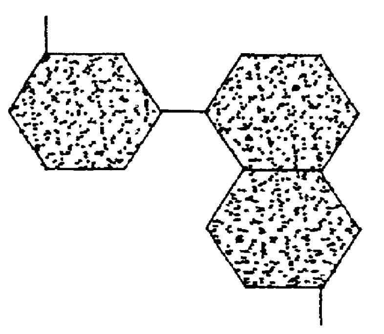
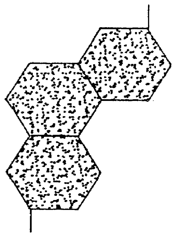
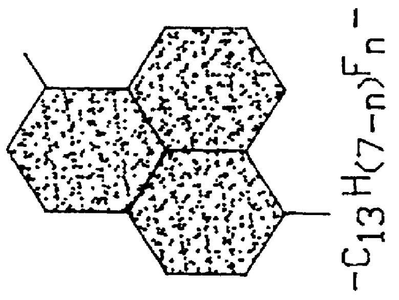
Image

Examples
example 1
Deposition of Siloxane Polymer Film
The parallel plate plasma system with magnetic confinement was used for polymerization of {Si--(OCH.sub.3).sub.2 }.sub.4 on a 4 inch diameter wafer. The power level was set at 80 Watts, the precursor flow rate was set at 75 SCCM, the deposition time was 20 minutes, and the deposition rate was 0.08.mu. / min. The film had a K of 2.32, Tg was 240.degree. C., and the residual stress on silicon substrate was 37 MPa.
example 2
Deposition of Siloxane Hydrocarbon Polymer Film
The plasma system described in Example 1 above was used for polymerization of an admixture of 60 molar % of {Si--(OCH.sub.3).sub.2 }.sub.4 and 40 molar % of CF.sub.3 --C.sub.6 H.sub.4 --CF.sub.3. The power level was set at 200 Watts, the precursor flow rate was set at 90 SCCM, the deposition time was 20 minutes, the deposition rate was 0.12 .mu.m / min. The film had a K of 2.21, a Tg of 310.degree. C., and a residual stress on a silicon substrate of 40 MPa.
example 3
Co-Polymerization of a Siloxane Hydrocarbon Polymer Film
The plasma system described in Example 1 above was used for polymerization of an admixture of 40 molar % of {Si--(OCH.sub.3).sub.2 }.sub.4 and 60 molar % of CF.sub.3 --C.sub.6 H.sub.4 --CF.sub.3. The power level was set at 200 Watts, the precursor flow rate was set at 90 SCCM, the deposition time was 20 minutes, the deposition rate was 0.12 .mu.m / min. The film had a K of 2.21, a Tg of 310.degree. C., and a residual stress on a silicon substrate of 32 MPa.
The foregoing descriptions and Examples are included for illustrative purposes only, and are not intended to limit the scope of the invention. Other features, aspects and objects of the invention can be obtained from a review of the figures and the claims. It is to be understood that other embodiments of the invention can be developed and fall within the spirit and scope of the invention and claims.
Incorporation of Reference
Each of the references cited above in this application...
PUM
| Property | Measurement | Unit |
|---|---|---|
| dielectric constant | aaaaa | aaaaa |
| diameter | aaaaa | aaaaa |
| vacuum pressure | aaaaa | aaaaa |
Abstract
Description
Claims
Application Information