Transparent electromagnetic wave shield

a technology of electromagnetic wave shielding and transparent material, which is applied in the direction of instruments, other domestic objects, synthetic resin layered products, etc., can solve the problems of unsuitable materials for light permeability use, difficult to maintain a stable electromagnetic wave shielding effect for a long time, and ineffective composite oxide in preventing leakage of electromagnetic waves, etc., to achieve disadvantageous weight and transparency, prevent irregular reflection, and increase strength

Inactive Publication Date: 2001-04-03
SUMITOMO BAKELITE CO LTD
View PDF7 Cites 47 Cited by
  • Summary
  • Abstract
  • Description
  • Claims
  • Application Information

AI Technical Summary

Benefits of technology

It has been considered as a standard that the allowable shielding effect of the conventional electromagnetic wave absorbers be at the level of 20 dB or above, which corresponds to an electromagnetic wave absorption rate of 99% or above, but according to the present invention it has become possible to raise the level of allowable shielding effect to 30-50 dB.
The transparent polymer reinforcing sheet can endure external pressure, but damage due to scratching or the like causes reduction of transparency, so that a protective hard coat may be provided as desired. Such a hard coat may be formed with thermosetting resins, for example, UV-curing resins such as epoxy acrylates and urethane acrylates, and epoxy resins. Inorganic materials, specifically transparent oxides such as silicon oxide, alumina, titanium oxide and zirconium oxide are also prefer

Problems solved by technology

With rapid progress of electronics and consequential prevalence of computers and other electronic devices in recent years, concern is growing over disturbance caused by electromagnetic waves which would generate erroneous operation of electronic devices.
Various materials such as metal foil, punched metal foil, metal mesh, metal fiber, plated organic or inorganic fiber, etc., have been used or tried for preventing leakage of electromagnetic waves, but transparency is an absolute requirement for the displays such as PDP and see-through windows, and any of said materials was unsuited for use from the aspect of light permeability.
Further, since oxidation proceeds on the metal surface with the lapse of time, even metal mesh which, among said materials, is considered to be best suited for meeting the transparency requirement, has the problem that high frequency contact tends to break at the lattice points, making it difficult to maintain a stable electromagnetic wave shielding effect for a long time.
It has also been conceived to use a composite oxide of indium oxide and tin oxide (hereinafter referred to as ITO) which is proof against oxidative degradation and widely used as electrode for liquid crystal displays, but it is rep

Method used


Image

  • Transparent electromagnetic wave shield
  • Transparent electromagnetic wave shield
  • Transparent electromagnetic wave shield

Examples


examples 2 and 3

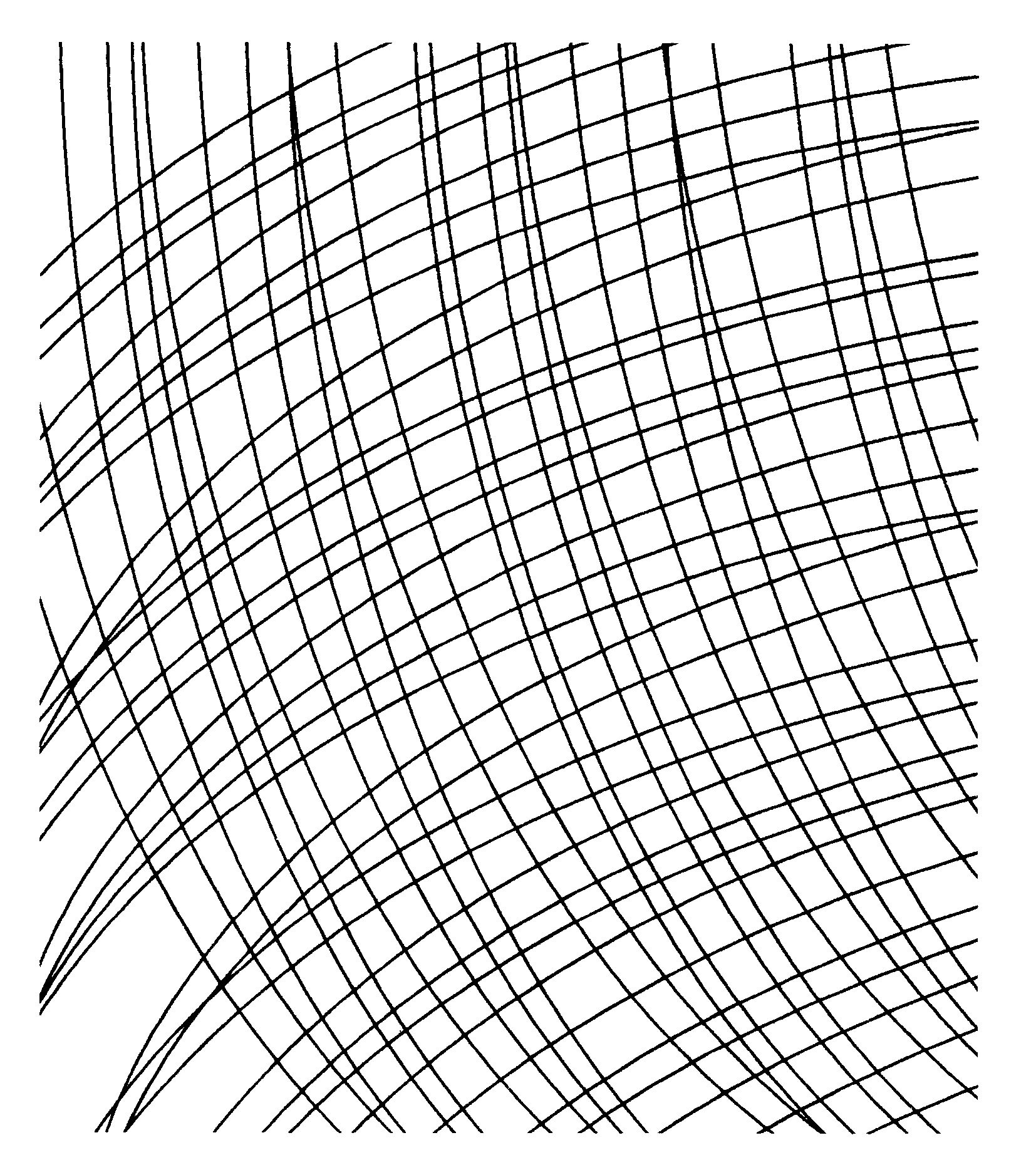
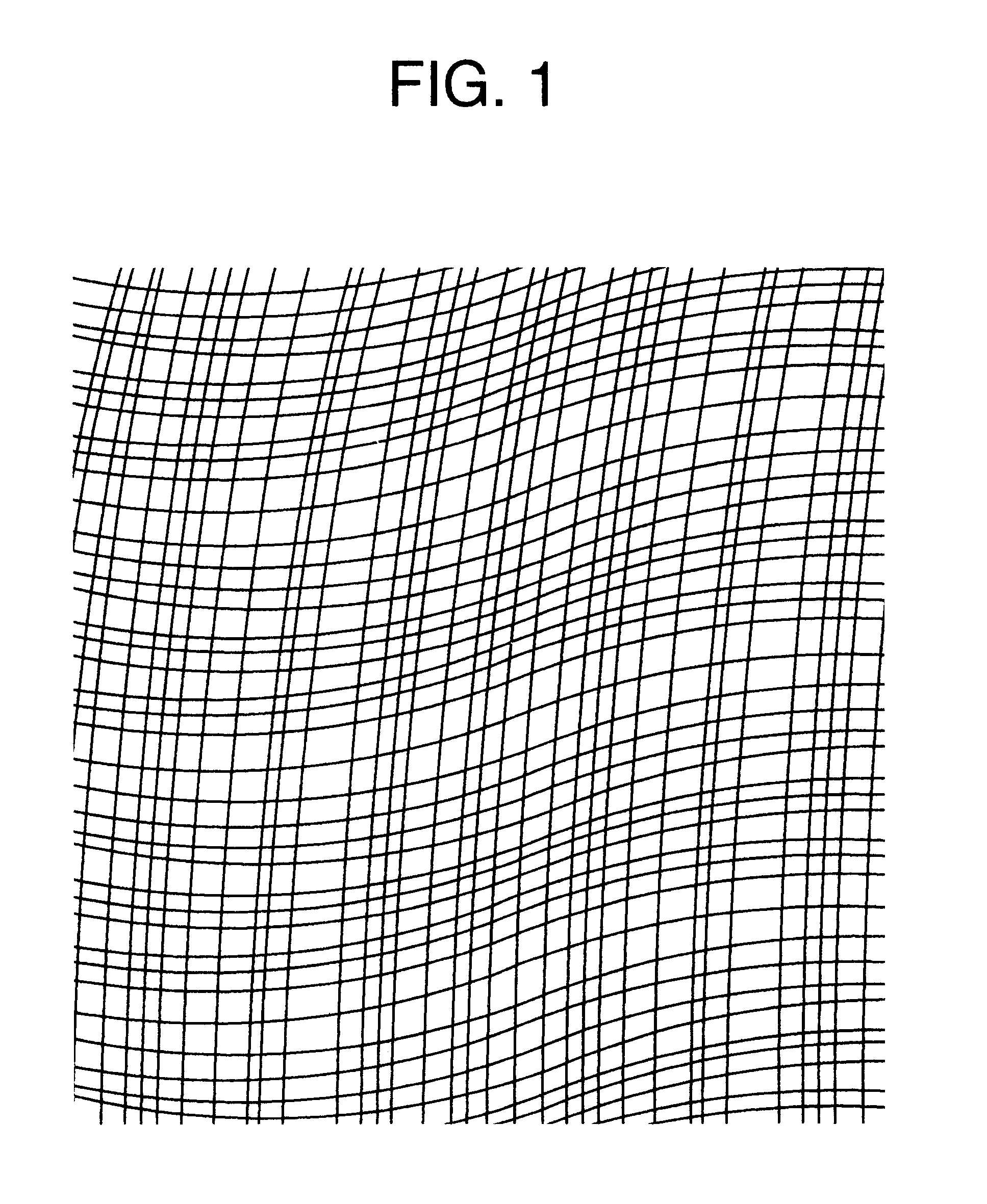
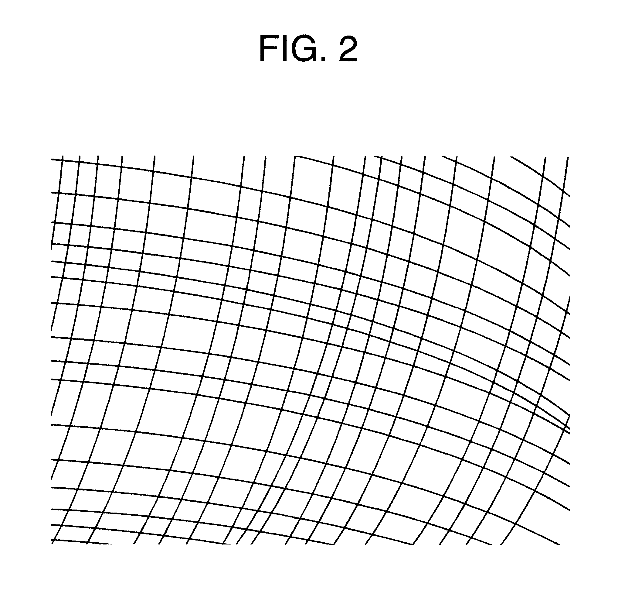
A polyurethane adhesive layer 1 was coated on a 75 .mu.m thick PET film, and then a copper foil (12 .mu.m thick) was laminated thereon to obtain a copper-foiled PET film. The conductive layer was patterned by photolithography to form a pattern comprising longitudinal and lateral array of curves expressed by Sin and Tan functions. The line width of the pattern was 10 .mu.m. The pitch of the lines was set according to the above-shown equation (6) (Example 2) and the following equation (7) (Example 3).

Pi=100+(170-150).times..alpha.i (7)

(.alpha.i: random number between 0 and 1)

Then, on one side of a 2 mm thick polycarbonate substrate was applied an antireflection hard coat with a pencil hardness of 3H or above, and the pattern-worked base film was laminated on the uncoated side of the polycarbonate substrate with an adhesive layer 2 of an aliphatic polyester-urethane (AD-N401 produced by TOYO-MORTON Co., Ltd.). A flat cable was bonded to the conductive layer at an outer edge with a silv...

examples 4-6

In Example 1, the pattern was formed with the curves expressed by an exponential function (Example 4), a logarithmic function (Example 5) and an inversely proportional function (Example 6). There were obtained the transparent electromagnetic wave shields which, when superposed on a PDP screen, caused no formation of moire fringe and provided excellent recognizability.

example 7

A 75 .mu.m thick PET film was undercoated to a thickness of 1 .mu.m with a coating material comprising 100 parts by weight of an epoxy acrylate prepolymer (VR-60 produced by Showa Kobunshi KK) having a molecular weight of 1,540 and a melting point of 70.degree. C., 400 parts by weight of butyl acetate, 100 parts by weight of cellosolve acetate and 2 parts by weight of benzoin ethyl ether. Then indium oxide was sputtered thereon to form a crystalline film having a permeability of 80% and a sheet resistance of 150 .OMEGA.. On this film was further formed a 2,000 .ANG. thick copper film by sputtering, followed by electroplating to obtain a copper-foiled PET film having a copper thickness of 4 .mu.m and a surface resistance of 4.times.10.sup.-3 .OMEGA. / .quadrature.. Patterning was conducted on the conductive layer by photolithography using ferric nitrate as etching solution to obtain a filter pattern of the configuration described in Example 1.

The copper foil sides of the obtained films...


PUM

PropertyMeasurementUnit
Lengthaaaaaaaaaa
Thicknessaaaaaaaaaa
Fractionaaaaaaaaaa

Abstract

A transparent electromagnetic wave shield comprising a transparent polymer film and a conductive layer of a linear pattern shape formed on at least one side of said film, wherein the line intervals in said linear pattern are random between 20 mum and 1 mm.

Description

The present invention relates to surface covering for the screens of display devices, especially plasma displays (hereinafter abbreviated as PDP) which need to be guarded against leakage of electromagnetic waves, and for other transparent structures which are required to be capable of being seen through, for example, windows of a room where medical instruments are installed.With rapid progress of electronics and consequential prevalence of computers and other electronic devices in recent years, concern is growing over disturbance caused by electromagnetic waves which would generate erroneous operation of electronic devices. One means for preventing such electromagnetic wave disturbance is active shielding capable of confining the unnecessary electromagnetic waves at the source of generation, which can be realized, for instance, by designing the housing of the electronic device to be electroconductive. Various materials such as metal foil, punched metal foil, metal mesh, metal fiber,...

Claims


Application Information

Patent Timeline
IPC IPC(8): H05K9/00
CPCH05K9/0096Y10S428/93Y10S428/923Y10T428/24802Y10T428/2978Y10T428/2976Y10T428/298Y10T428/24995Y10T428/249952H05K9/00
Inventor GOTO, HIDEKITANAKA, JUNJI
Owner SUMITOMO BAKELITE CO LTD
Why Eureka
Try Eureka