

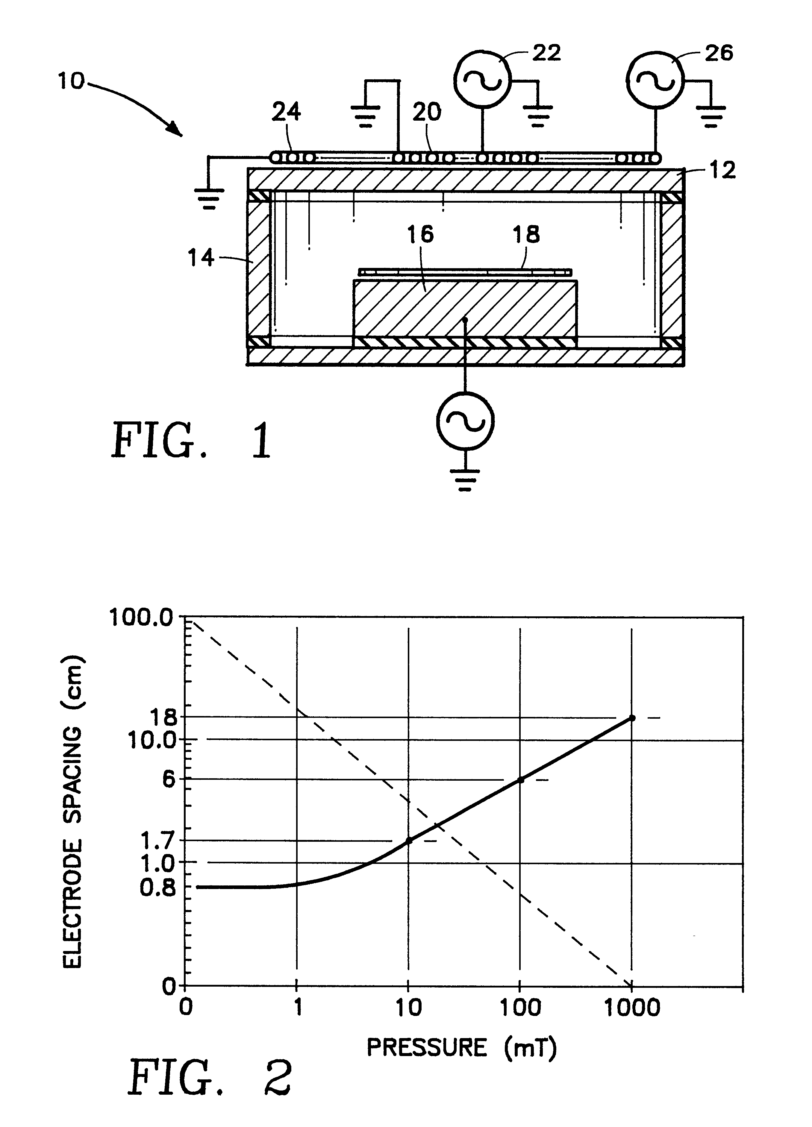
High pressure high non-reactive diluent gas content high plasma ion density plasma oxide etch process
a non-reactive diluent, plasma oxide technology, applied in plasma techniques, variable inductances, inductances, etc., can solve the problems of weakened polymer formation, limited selectivity, and inadequate etch selectivity of silicon dioxide to the underlying non-oxygen containing layer
- Summary
- Abstract
- Description
- Claims
- Application Information
AI Technical Summary
Benefits of technology
Problems solved by technology
Method used
Image

Examples
working example
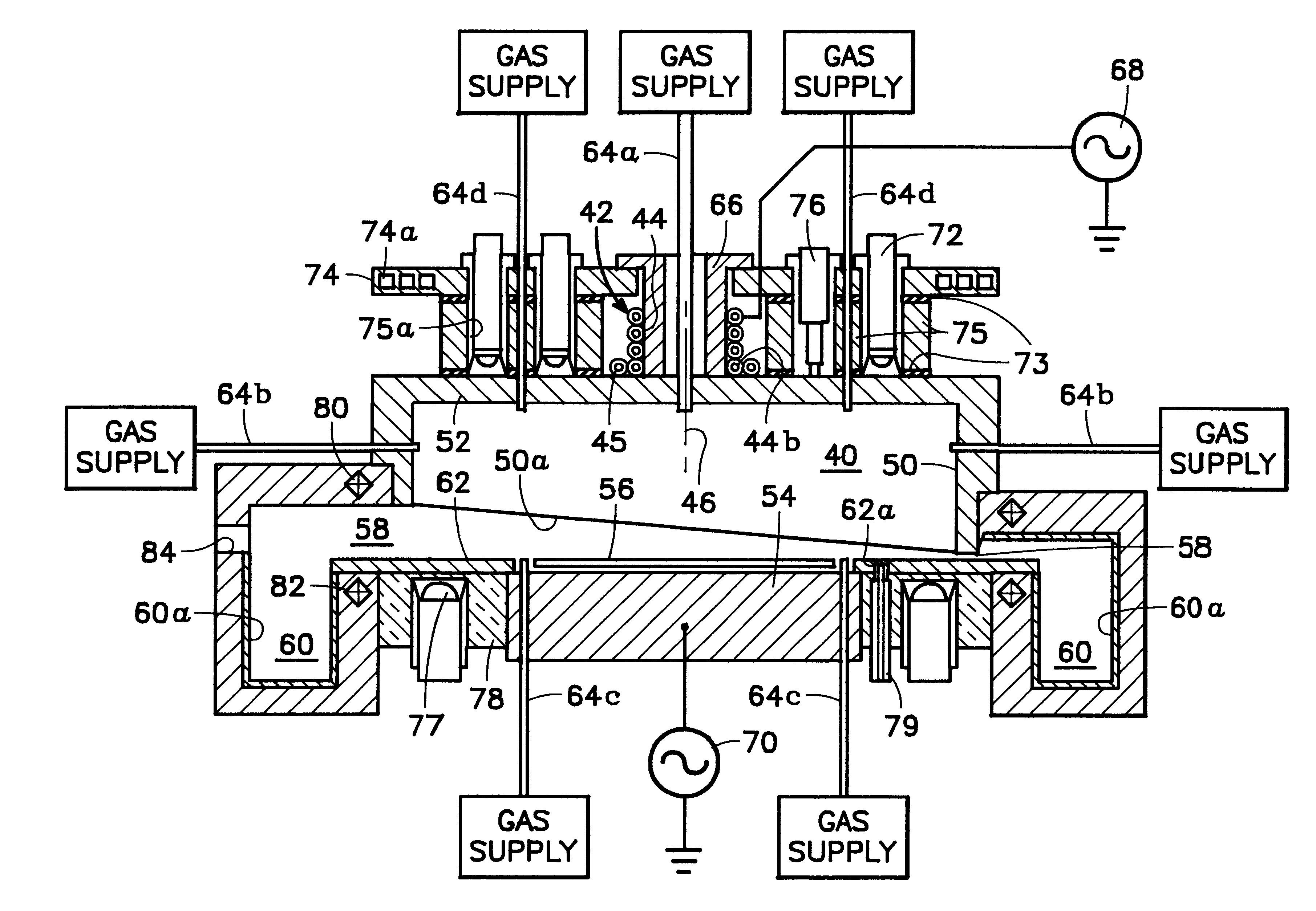
Reactor Parameter Settings:
CHF.sub.3 gas flow rate: 90 sccm
C.sub.4 F.sub.8 gas flow rate: 10 sccm
CO.sub.2 gas flow rate: 16 sccm
Ar gas flow rate: 450 sccm
total chamber pressure: 85-90 mTorr
chamber surface temperature: 1500.degree. C.
silicon ring temperature: 450.degree. C.
plasma volume: 6.5 liters
chamber volume: 22 liters
outer coil power: 3072 watts @ 2.0 MHz
inner coil power: 1178 watts @ 2.3 MHz
bias power to pedestal: 1600 watts @ 1.8 MHz
wafer on electrostatic chuck at -10.degree. C. w / helium cooling gas
In this example, a vacuum pump which pumped down the chamber pressure was a conventional turbopump of the type having a nominal capacity of 1000 liters / second with a net flow rate of 300 liters / second at a chamber pressure of 10 mT and a net flow rate of 110 liters / second at a chamber pressure of 100 mT. A throttle valve at the pump intake from the chamber was 18% open in this example.
Results:
(1) deep oxide contact holes etched at 0.4 micron diameter at approximately 10,000 angstrom...
PUM
| Property | Measurement | Unit |
|---|---|---|
| height | aaaaa | aaaaa |
| height | aaaaa | aaaaa |
| phase angle | aaaaa | aaaaa |
Abstract
Description
Claims
Application Information