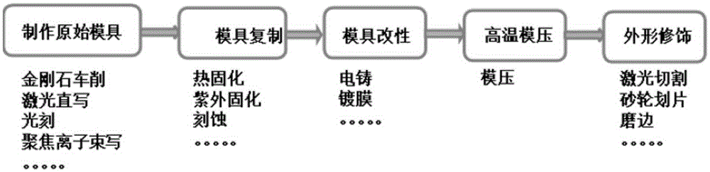
Method for manufacturing inorganic micro-optical elements in batches
A manufacturing method and micro-optical technology, which are applied in micro-structure technology, gaseous chemical plating, micro-structure devices, etc., can solve the problems such as the inability to realize the batch size and high efficiency of arrayed inorganic micro-optical elements, and achieve low cost, high efficiency, etc. Improved wear resistance and thermal stability
- Summary
- Abstract
- Description
- Claims
- Application Information
AI Technical Summary
Problems solved by technology
Method used
Image

Examples
Embodiment 1
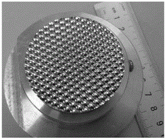
[0020] Example 1: Mass production of inorganic glass micro-cylindrical lenses:
[0021] (1) Use the Y-axis cutting function of the diamond lathe or the flying knife cutting function to process the PMMA micro-cylindrical lens array, the micro-cylindrical lens is 225um deep, the diameter is 1mm, the long Y-axis movement speed is 200mm / min, and the Z-axis roughing feed is 5 ~40um each time, the fine turning feed is 1~10um each time, the rough turning X axis feed is 5~20um per step, the fine turning X axis feed is 1~3um per step.
[0022] (2) The original mold of the diamond-turned cylindrical lens array is used for PDMS replication, the ratio of PDMS and curing agent is 10:1, and the product is baked in a vacuum oven at 80 degrees for 30 minutes.
[0023] (3) Copy the PDMS mold into a photosensitive glue pattern through ultraviolet curing photosensitive glue, the photosensitive glue model is NOA68, and the illumination intensity is 10mW / cm 2 , Fixed time 15min.
[0024] (4) Use photosens...
Embodiment 2
[0027] Embodiment 2: Inorganic micro lens array, the implementation steps of the invention are:
[0028] (1) Use laser direct writing equipment to directly produce continuous surface microlens array on photoresist. The microlens array has a diameter of 400um and a height of 10um. Using a 2mm laser direct write head, program MATLAB to obtain grayscale graphics and input laser Direct writing system for continuous surface structure processing.
[0029] (2) Adopting plasma dry etching process, using two gases of trifluoromethane and sulfur hexafluoride, etching power 80W~150W, etching for 8 hours.
[0030] (3) Use the dry-etched microlens array mold for electroforming, the electroforming current density is not more than 5A.h / dm 2 , The thickness of the electroformed plate is greater than 2mm, and then a 50nm thick SiC film is grown on the patterned surface of the nickel plate by magnetron sputtering.
[0031] (4) Assemble the nickel micro-lens array mold and the glass substrate and place ...
Embodiment 3
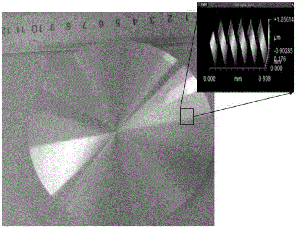
[0033] Example 3: Mass production of inorganic planar diffractive optical elements. The implementation steps of the invention are:
[0034] (1) Using photolithography technology, make a diffraction grating structure with a feature size of 10um or less, and use the process steps of glue coating, pre-baking, exposure, and development to make a photoresist diffraction grating mold.
[0035] (2) Use the photoresist diffraction grating mold for electroforming, the electroforming current density is not more than 5A.h / dm 2 , The thickness of the electroformed plate is greater than 2mm, and then a 50nm thick SiC film is grown on the patterned surface of the nickel plate by magnetron sputtering.
[0036] (3) Assemble the nickel diffraction grating mold and the glass substrate on the tablet press table in the molding press, and gradually increase the temperature from 300℃ to 600℃. The heating adopts multi-station step-by-step heating, and each station is heated for 1-10min. Apply pressure to t...
PUM
 Abstract
Description
Claims
Application Information