VGF/VB gallium arsenide single-crystal furnace structure and growing method

A growth method and technology of gallium arsenide, applied in the field of semiconductor material preparation, can solve problems such as disadvantages, and achieve the effects of preventing deformation, increasing crystallization rate, and improving degree of depression

Inactive Publication Date: 2019-01-22
CHINA ELECTRONICS TECH GRP NO 46 RES INST
View PDF13 Cites 26 Cited by
  • Summary
  • Abstract
  • Description
  • Claims
  • Application Information

AI Technical Summary

Problems solved by technology

On the contrary, it is not conducive to the growth of silicon-doped low-resistance gallium arsenide single crystal

Method used


Image

  • VGF/VB gallium arsenide single-crystal furnace structure and growing method
  • VGF/VB gallium arsenide single-crystal furnace structure and growing method

Examples


Embodiment 1

[0044] Embodiment 1: 4-inch carbon-doped semi-insulating gallium arsenide single crystal growth.

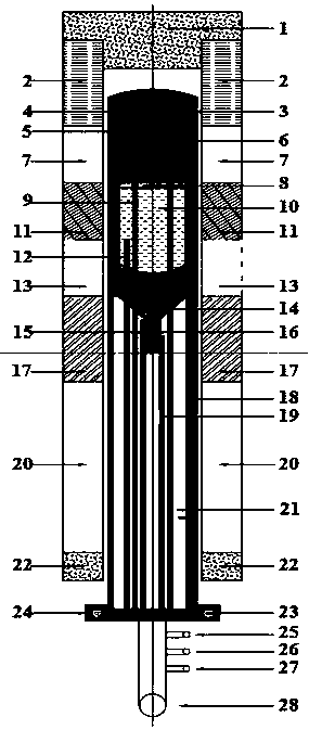
[0045] The quartz tube 3 used had an inner diameter of 130 mm, a thickness of 8 mm, and a length of 120 mm.

[0046] First load ) crystal orientation seed crystal, then load 80g of boron oxide with water content less than 200ppm, and then load D-type gallium arsenide polycrystal synthesized by horizontal method or gallium arsenide with a diameter of 100mm synthesized by high-voltage VGF Polycrystalline 8.3±0.1kg. Then place it on the graphite support base 21, cover the quartz tube 3, seal the quartz tube 3 and the stainless steel flange 24 with water cooling. With water-cooled stainless steel flange 24, the external six monitoring thermocouple quick-plug connectors are connected to the compensation wires of the temperature control system, connected to the flange for circulating cooling water, vacuuming and inflation and deflation pipelines, in manual mode, lift with water-cooled...

Embodiment 2

[0053] Embodiment 2: The differences between this embodiment and Embodiment 1 are: (1) 4-inch Si-doped low-resistance gallium arsenide single crystal growth. First load the crystal orientation seed crystal, then load 80g of boron oxide with a water content less than 200ppm, and then load D-type gallium arsenide polycrystal synthesized by horizontal method or gallium arsenide polycrystal with a diameter of 100mm synthesized by high-voltage VGF 10 ±0.3kg, loaded with 1±0.05g of silicon chip with resistivity above 1000Ω•cm. (2) After vacuuming, only fill with argon to 0.35MPa. (3) The VB growth stroke is 200mm for the crystal. (4) VB drop speed 2.0mm / h.

[0054] Cut a test piece from the crystal head to tail to test the low resistance GaAs carrier concentration, resistivity and dislocation density. The test crystal head and tail parameters are shown in Table 2.

[0055] Table 2

[0056] Diameter control (mm)

Embodiment 3

[0057] Embodiment 3: The difference between this embodiment and Embodiment 1 is: (1) A 6-inch growth single crystal furnace consisting of a graphite support base, a quartz tube and a water-cooled stainless steel flange is used to grow a 6-inch carbon-doped semi-insulating arsenic Gallium single crystal. The quartz tube 3 used had an inner diameter of 179 mm, a thickness of 10 mm, and a length of 120 mm. (2) First load ) crystal orientation seed crystal, then load 150g of boron oxide with water content less than 200ppm, and then load D-type gallium arsenide polycrystal synthesized by horizontal method or gallium arsenide with a diameter of 150mm synthesized by high-voltage VGF Polycrystalline 16±0.1kg. (3) After vacuuming, fill with argon to 0.30MPa, and then fill with CO to 0.4MPa. (4) The VB growth stroke is 150mm for the crystal. (5) VB drop speed 1.0mm / h.

[0058] After the crystal is heat-treated, a test piece is cut from the crystal head and tail, and the semi-insulat...


PUM

PropertyMeasurementUnit
thicknessaaaaaaaaaa
lengthaaaaaaaaaa
thicknessaaaaaaaaaa

Abstract

The invention discloses a VGF / VB gallium arsenide single-crystal furnace structure and a growing method. According to the VGF / VB gallium arsenide single-crystal furnace structure, a resistance heatingfurnace which is relatively lowest in production cost and is provided with multiple temperature zones is adopted; a support structure adopts graphite; the support strength is improved; the loading amount is favorably increased; release of latent heat of growth crystallization is facilitated; the crystal yield of crystal growth is favorably improved; a sealing structure with a reusable quartz tubeand a stainless steel flange is adopted; a 1-atm air charging and discharging automatic valve is additionally arranged on an air channel pipeline, so that the balance of inner air pressure and outerair pressure of the quartz tube can be effectively guaranteed, and the influence of deformation of the quartz tube on reuse is avoided. A VGF method and a VB method are used for growing crystals; whenthe crystals are grown by the VB method, the sunken degree of a concave solid-liquid interface of the VGF growth method can be improved, so that the crystal yield is favorably improved. The single-crystal furnace and the growth method are used for growing the gallium arsenide single crystals with maximum size of 8 inches; meanwhile, the quartz tube can be reused, so that the production cost can be reduced; a CO atmosphere doping manner also can be used for controlling the resistivity and the axial resistivity uniformity of semi-insulating gallium arsenide.

Description

technical field [0001] The invention relates to a semiconductor material preparation technology, in particular to a VGF / VB gallium arsenide single crystal furnace structure and a growth method. Background technique [0002] Gallium arsenide has a direct band gap (1.42eV), high electron mobility (8500cm 2 / V·s), high electron saturation drift speed and other characteristics. These characteristics determine that microelectronic devices such as high frequency, high speed, high temperature and radiation resistance are widely used in radar, satellite TV broadcasting, microwave and millimeter wave communication, wireless communication (representative of mobile phone) and optical fiber communication. The direct bandgap characteristic determines that gallium arsenide can also be used in optoelectronic fields such as optical communication active devices (LD), red and yellow light-emitting diodes (LED), visible light lasers, near-infrared lasers, quantum well high-power lasers, and h...

Claims


Application Information

Patent Timeline
Patent Type & Authority Applications(China)
IPC IPC(8): C30B29/42C30B11/00
CPCC30B11/00C30B11/006C30B29/42
Inventor 周春锋兰天平边义午王东兴
Owner CHINA ELECTRONICS TECH GRP NO 46 RES INST
Why Eureka
Try Eureka