A single-sided texturing process for monocrystalline silicon wafers and a method for preparing solar cells

A single-side texturing and monocrystalline silicon wafer technology, which is applied in the direction of single crystal growth, single crystal growth, chemical instruments and methods, etc., can solve the problem of affecting the quality of single crystal PERC cells, the flatness of the back polishing surface is not ideal, and the cell In order to improve the battery efficiency and quality, save texturing chemicals, and improve the flatness of the back passivation, etc.

Active Publication Date: 2022-01-28
正泰新能科技股份有限公司
View PDF5 Cites 0 Cited by
  • Summary
  • Abstract
  • Description
  • Claims
  • Application Information

AI Technical Summary

Problems solved by technology

[0005] Single crystal texturing has been relatively perfect, and is widely used in various cell manufacturers. At present, there is still an unsatisfactory problem in the flatness of the back polishing surface in the second cleaning process, which leads to poor post-passivation effect of the cell, which seriously affects the single crystal PERC battery quality

Method used


Image

  • A single-sided texturing process for monocrystalline silicon wafers and a method for preparing solar cells

Examples


preparation example Construction

[0051] The present invention also provides a method for preparing a solar cell, comprising the following steps:

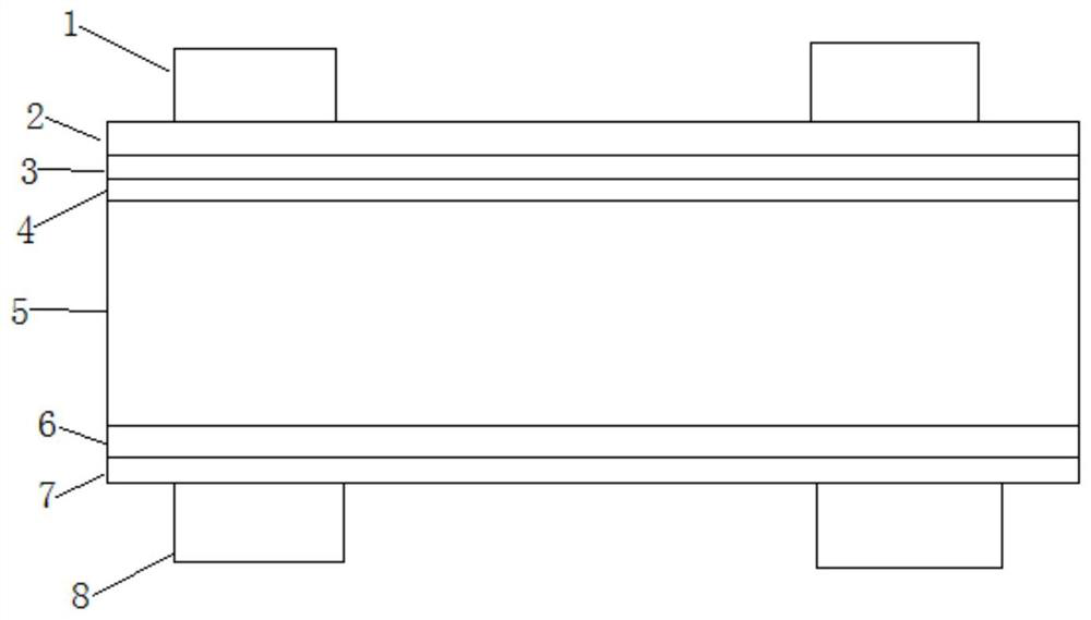
[0052] 1) Prepare a phosphorous diffusion layer and a silicon dioxide tunneling layer sequentially on the front side of the above-mentioned front textured monocrystalline silicon wafer,

[0053] 2) depositing an aluminum oxide layer on the back side of the monocrystalline silicon wafer obtained in the step 1);

[0054] 3) depositing a silicon nitride layer with a thickness of 60 to 90 nm on the front side of the monocrystalline silicon wafer obtained in step 2);

[0055] 4) Depositing a silicon nitride layer with a thickness of 100-150 nm on the back side of the monocrystalline silicon wafer obtained in step 3)

[0056] 5) performing laser drilling on the back of the monocrystalline silicon wafer obtained in step 4), and then sintering the screen to obtain a solar cell.

[0057] The present invention carries out phosphorus diffusion on the textured surface (i.e. ...

Embodiment 1

[0068] Add resin, cellulose, additives, and nano-silica powder in a certain proportion, heat and stir at 60°C for 5 minutes, and prepare a solution-like colloid (mass ratio of silica powder: additive: cellulose: resin = 1:1:0.5: 15.

[0069] Place the P-type monocrystalline silicon wafer on the tray of the spin-coating instrument, drop mask glue on the back surface of the silicon wafer, and spin-coat to prepare a mask glue with a thickness of 2 μm;

[0070] For texturing, use potassium hydroxide solution for texturing, and use 10% HF aqueous solution to wash off the mask glue after texturing;

[0071] Phosphorus diffusion to obtain a phosphorus diffusion layer with a square resistance of 130Ω / □ to form an N+ emitter;

[0072] Use etching equipment to remove phospho-silicate glass and polish the back surface; since the back surface does not participate in the texturing reaction, no pyramid-like texture is formed, and the back surface is relatively flat compared with convention...

Embodiment 2

[0080] Add resin, cellulose, additives, and nano-silica powder in a certain proportion, heat and stir at 60°C for 5 minutes, and prepare a solution-like colloid (mass ratio of silica powder: additive: cellulose: resin = 0.5:1:0.5: 20.

[0081] Place the P-type monocrystalline silicon wafer on the tray of the spin-coating instrument, drop the mask glue on the back surface of the silicon wafer, and spin-coat to prepare a mask glue with a thickness of 1 μm;

[0082] For texturing, use potassium hydroxide solution for texturing, and use 10% HF aqueous solution to wash off the mask glue after texturing;

[0083] Phosphorus diffusion to obtain a phosphorus diffusion layer with a square resistance of 110Ω / □, forming an N+ emitter;

[0084] Use etching equipment to remove phospho-silicate glass and polish the back surface; since the back surface does not participate in the texturing reaction, no pyramid-like texture is formed, and the back surface is relatively flat compared with con...


PUM

PropertyMeasurementUnit
thicknessaaaaaaaaaa
thicknessaaaaaaaaaa
thicknessaaaaaaaaaa

Abstract

The invention provides a single-side texturing process for a single-crystal silicon wafer, comprising the following steps: A) coating a mask glue solution on the back side of a single-crystal silicon wafer to obtain a single-crystal silicon wafer with a mask coating on the back ; The mask glue solution includes the following components in parts by weight: silicon oxide: 0.1-1 parts, additives: 0.5-2 parts, lignin fiber: 0.1-1 parts, gum arabic: 10-100 parts; B ) pickling the monocrystalline silicon wafer with a mask coating on the backside after texturing in an alkaline reagent, removing the mask coating, and obtaining a monocrystalline silicon wafer textured on one side. The invention uses silicon oxide and resin as the main components, and can prepare a mask coating at a very low temperature, with low energy consumption. Resin and silicon oxide play the role of blocking and masking, and the blocking effect is better. Silicon oxide In addition to acting as a mask, it also plays a role in helping to dissolve the subsequent mask removal.

Description

technical field [0001] The invention belongs to the technical field of photovoltaic solar cells, and in particular relates to a single-side texturing process of a monocrystalline silicon chip and a preparation method of a solar cell. Background technique [0002] At present, batteries in the photovoltaic industry can be divided into crystalline silicon solar cells and thin-film solar cells according to different substrate materials. Among them, the development of crystalline silicon solar cells is relatively mature, and there is still a lot of room for improvement in cost and efficiency. It is the mainstream of the current market. The number of free electrons and holes that pure crystalline silicon can generate is far from meeting the needs of photovoltaic power generation. Therefore, the commonly used technology is to dope pure silicon, doping phosphorus in it to form an N-type semiconductor, in which Doping with boron element forms a P-type semiconductor. [0003] Current...

Claims


Application Information

Patent Timeline
Patent Type & Authority Patents(China)
IPC IPC(8): C30B33/10C30B29/06C23C16/50C23C16/34C30B31/00C23C16/455C23C16/40H01L31/0236H01L31/18
CPCC30B33/10C30B29/06C23C16/50C23C16/345C30B31/00C23C16/45525C23C16/403H01L31/1804H01L31/02366Y02E10/547Y02P70/50
Inventor 马玉超余浩张晓攀单伟何胜徐伟智
Owner 正泰新能科技股份有限公司
Why Eureka
Try Eureka