
Monocrystalline silicon wafer texturing additive and application thereof

A single crystal silicon wafer and additive technology, which is applied in the direction of single crystal growth, single crystal growth, sustainable manufacturing/processing, etc., can solve the problems of large environmental impact, low speed, high cost, etc.

Inactive Publication Date: 2021-05-18
INST OF CHEM ENG GUANGDONG ACAD OF SCI
View PDF6 Cites 4 Cited by
  • Summary
  • Abstract
  • Description
  • Claims
  • Application Information

AI Technical Summary

Problems solved by technology

Compared with diamond wire cutting, the rate of mortar cutting is low, and a large amount of mortar will be generated due to abrasion during the cutting process, which needs to be recycled and has a relatively large impact on the environment, which leads to the cost ratio of mortar cutting monocrystalline silicon wafers. Diamond wire cutting is relatively high, so companies generally prefer to use diamond wire-cut monocrystalline silicon wafers for texturing

Method used


Image

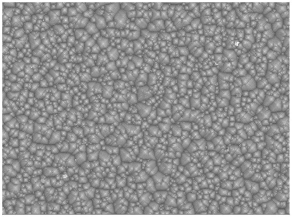
  • Monocrystalline silicon wafer texturing additive and application thereof
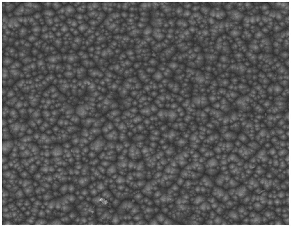
  • Monocrystalline silicon wafer texturing additive and application thereof
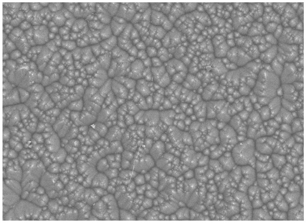
  • Monocrystalline silicon wafer texturing additive and application thereof

Examples


Embodiment 1

[0039] Embodiment 1 of the present invention: the application of a kind of monocrystalline silicon slice texturing additive, comprises the following steps:

[0040] S1. Preparation of monocrystalline silicon wafer texturing additives: 0.03g polyethylene glycol-600, 1.0g polyethylene glycol-400, 0.3g sodium carboxymethylcellulose, 1.0g potassium perfluorooctanesulfonate, 0.5 gN, N-methylenebisacrylamide, 0.8g gallic acid, 0.5g triethylene glycol monobutyl ether and 0.5g sodium benzoate were added to water to prepare 100g monocrystalline silicon chip texturing additive.

[0041] S2. Prepare monocrystalline silicon wafer texturing liquid: Add monocrystalline silicon wafer texturing additive to sodium hydroxide solution (mass fraction: 1.5%) to obtain monocrystalline silicon wafer texturing liquid; wherein, the texturing additive and hydrogen The volume ratio of sodium oxide solution is 0.8:100.

[0042]S3, cashmere making: sodium hydroxide solution, hydrogen peroxide solution an...

Embodiment 2

[0043] Embodiment 2 of the present invention: the application of a monocrystalline silicon wafer texturing additive, comprises the following steps:

[0044] S1. Preparation of monocrystalline silicon wafer texturing additives: 0.0005g of alkyl glucoside, 1.5g of polyethylene glycol-200, 0.5g of sodium alginate, 0.3g of tetraethylammonium perfluorohexylsulfonate, 10.0g of N-methyl Pyrrolidone, 0.3g of gallic acid, 0.6g of diethylene glycol monobutyl ether, 0.5g of sodium benzoate were added to water to prepare 100g of a monocrystalline silicon chip texturing additive.

[0045] S2. Preparation of monocrystalline silicon wafer texturing liquid: Add monocrystalline silicon wafer texturing additive to sodium hydroxide solution (2.0% by mass fraction) to obtain monocrystalline silicon wafer texturing liquid; wherein, the texturing additive and hydrogen The volume ratio of sodium oxide solution is 0.6:100.

[0046] S3, cashmere making: sodium hydroxide solution, hydrogen peroxide so...

Embodiment 3

[0047] Embodiment three of the present invention: the application of a monocrystalline silicon chip texturing additive, comprises the following steps:

[0048] S1. Preparation of monocrystalline silicon wafer texturing additives: 1.0 g polyethylene glycol-400, 3.0 g polyethylene glycol-200, 0.3 g sodium carboxymethyl cellulose, 0.3 g perfluorooctyl ammonium sulfonate, 10.0 gN-methylpyrrolidone, 0.05gN-N-methylenebisacrylamide, 0.5g gallic acid, 0.7g diethylene glycol monobutyl ether and 0.3g sodium benzoate, add water to make 100g monocrystalline silicon chip texturing additive .

[0049] S2. Preparation of monocrystalline silicon wafer texturing liquid: adding monocrystalline silicon wafer texturing additive to potassium hydroxide solution (mass fraction: 1.5%) to obtain monocrystalline silicon wafer texturing liquid; wherein, the texturing additive and hydrogen The volume ratio of potassium oxide solution is 0.8:100.

[0050] S3, cashmere making: sodium hydroxide solution,...


PUM

PropertyMeasurementUnit
sizeaaaaaaaaaa
quality scoreaaaaaaaaaa

Abstract

The invention discloses a monocrystalline silicon wafer texturing additive and application thereof. The texturing additive comprises the following raw materials: a nonionic surfactant, an amide compound, a perfluorinated ionic surfactant, a carbohydrate, gallic acid, ethylene glycol butyl ether and benzoate. The texturing additive can be used for well preparing pyramids which are uniform in size and range from 2 microns to 5 microns. According to the invention, compounding is carried out through the synergistic effect of the surfactants, dependence on isopropyl alcohol (IPA) in a traditional production process is eliminated, the alcohol-free texturing additive is prepared, and the production cost of the process and harm of toxic isopropyl alcohol steam volatilization to a human body are greatly reduced.

Description

technical field [0001] The invention relates to the field of manufacturing silicon wafers of solar cells, in particular to a texturing additive for monocrystalline silicon wafers and an application thereof. Background technique [0002] In order to prepare high-performance and efficient solar cells, it is first necessary to perform texturing on the surface of single-crystal silicon wafers. The texturing of monocrystalline silicon wafers generally uses a low-concentration alkaline etching solution to etch the silicon wafers, so that the surface of the silicon wafers forms a micron-scale pyramid-like suede structure, so the incident light can be reflected and refracted multiple times on it. It changes the direction of incident light in silicon, prolongs the optical path, and has excellent anti-reflection effect. In addition, due to the structural properties of the PN junction, the multiple internal reflections of the incident light on the surface of the silicon wafer can enha...

Claims


Application Information

Patent Timeline
Patent Type & Authority Applications(China)
IPC IPC(8): C30B33/10C30B29/06H01L31/0236H01L31/04H01L31/18
CPCC30B29/06C30B33/10H01L31/02363H01L31/04H01L31/1804Y02E10/50Y02P70/50
Inventor 喻桉史华红麦裕良文武
Owner INST OF CHEM ENG GUANGDONG ACAD OF SCI
Learn More