[0017] In accordance with a further aspect of the present disclosure the REDS layer (Rare-Earth Doped Semiconductor layer) is patterned to further define one or more
optical processing elements such as plural waveguides (WG's—or more specifically, Arrayed WaveGuides (AWG's) which can respectively process different wavelengths, thus providing
wavelength domain
multiplexing and demultiplexing), gratings, phase shift modulators, and optically, electrically and / or mechanically (e.g., MEM's) controlled spatial multiplexers and / or demultiplexers. With the use of
semiconductor-based
gain media (e.g.,
monocrystalline silicon that is appropriately doped with one or more
rare earth elements) instead of organic-based
gain media it becomes possible to provide stable and reliable optical amplification integrally with further
optical processing functions such as AWG's, etc. Thus, an integrated,
solid-state, planar optical device with good reliability and stability may be provided that can be used with electrical pump energy and / or optical pump energy—where the latter can be a
Raman pump or a non-
Raman pump. If a
Raman pump is used, the device may be structured to reshape (recondition) the optical information contained in the amplified beams, as generally would an O-E-O module that contains electrical amplification means, electrical signal reconditioning and optical
signal regeneration means.
[0018] In accordance with further aspects of the present disclosure it will be seen that non-organic materials such as
silicon and / or
silicon oxide and / or other semiconductors and / or their compounds can be integrally formed as part of a monolithic or other integrated device so as to define an optical gain media that is
erbium doped (Er-doped) for use, for example in the 1.5 μm transmission band; and / or that is doped with other
rare earth elements such as Nd+ or Yb+ doped for respective use in the 1.34 μm or 1.3 μm bands. Preparation methods for forming the rare earth doped
semiconductor regions may include surface
plasma deposition of the rare earth elements, and / or inclusion of the rare earth elements in vapor deposition processes (e.g., CVD, ALD, etc.) and / or
diffusion, and / or
ion implantation of the rare earth elements into the material regions that are to function as optical gain regions. Additionally, concentrations of the incorporated rare earth elements (e.g., Er) in their host materials (e.g., Si or SiO2) may be enhanced by use of respectively more-soluble rare earth compounds (e.g., ErO) that can form
solubility-enhancing complexes (e.g., Er—O—Si═Si═ . . . ) with their host materials. Additionally or alternatively, concentrations of the incorporated rare earth elements (e.g., Er) in their host materials (e.g., monocrystalline or polycrystalline Si or SiO2) may be enhanced by
trapping them under or between amorphous
layers (e.g., amorphous Si and / or
amorphous silicon oxide or
amorphous silicon nitride) so as to reduce out-
diffusion, particularly as a result of rare earth
dopant (e.g. Er) activation by
rapid thermal annealing or the like.
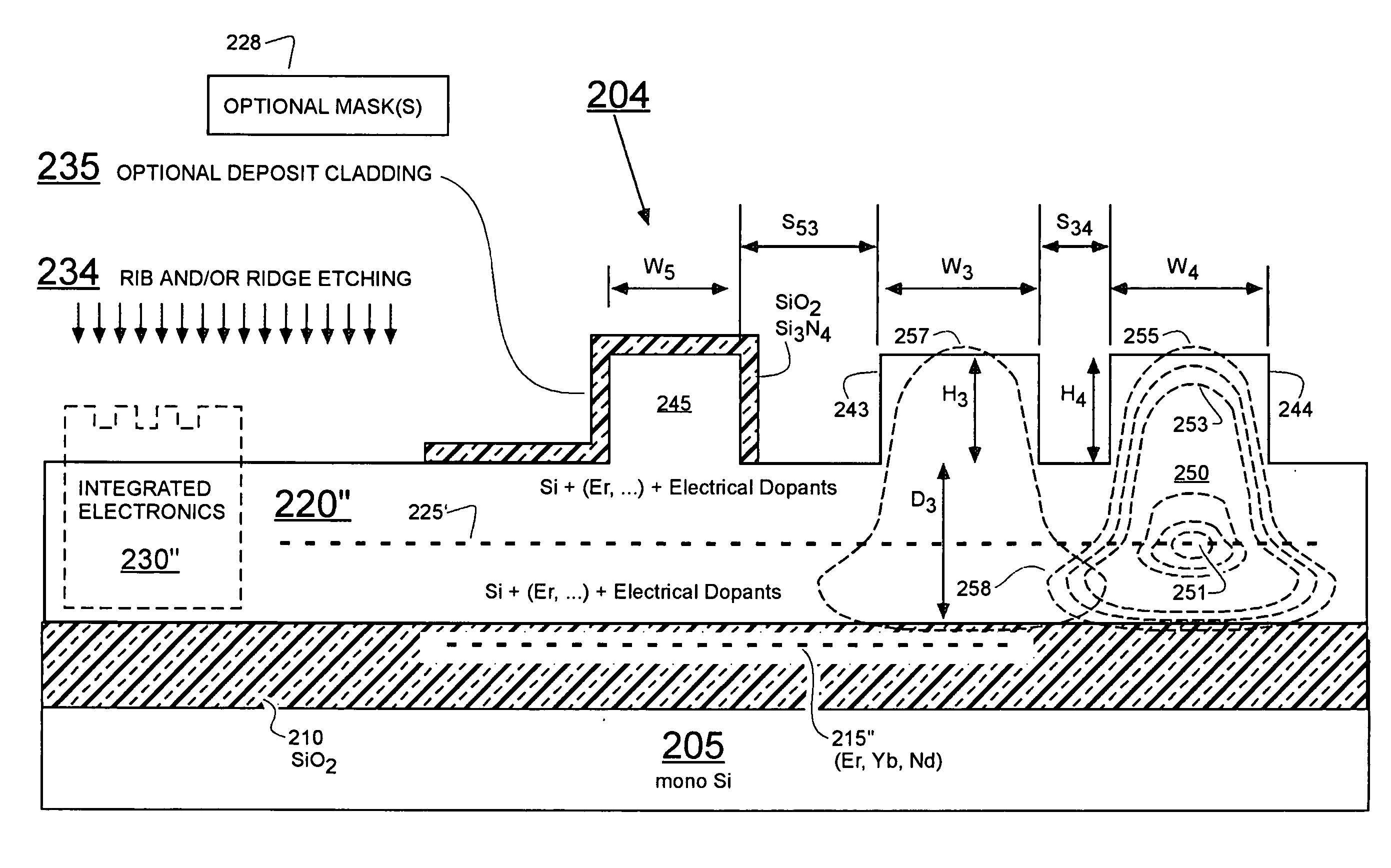
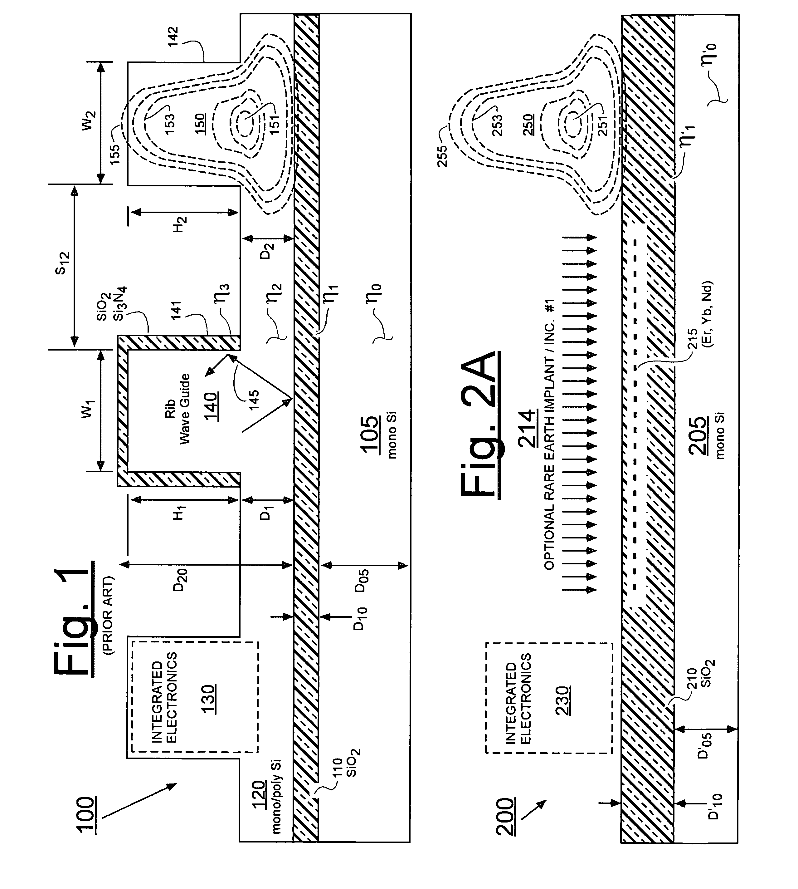
[0019] In accordance with further aspects of the present disclosure it will be seen that the optical gain regions may be integrated within
ridge waveguides,
rib waveguides and / or the like and that the latter may define amplifying waveguides, amplifying arrayed waveguides (AWG's), amplifying optical switches and other optical or electro-optical components of suitable small sizes that may be used for photonic integration applications. It will be seen that various optical gain-media pumping methods may be employed including
electrical current injection (for generating electrically excited
luminescence or
electroluminescence); use of 980 nm
laser pump and / or use of Raman pumping. It will be seen that various pump energy injection configurations may be used including: non-parallel injection (this including having the pumping beam travel in any direction other than parallel to, and in exactly the same direction as that of the
signal beam) and more specifically, having the pumping beam travel generally perpendicularly to the information-carrying,
signal beam and repeatedly bouncing the pumping beam back and forth in non-parallel fashion within the gain media so as to increase the number of signal-amplifying interactions occurring between the triad of the pumping beam, the
signal beam, and the available concentration of rare earth atoms. More specifically, metallic or other mirrors may be used to provide multiple internal reflection of the pump energy through the gain media to thereby increase pumping efficiency and reduce pump-to-
signal interference and to thereby produce an easily-extractable output signal beam that has improved
signal to noise ratio).
[0021] It will be seen that the integrally formed, optical-gain regions may be used to monolithically form
Erbium Doped Planar Amplifiers (EDPA's) or
Erbium Doped Planar Raman
Amplifier (EDPRA's) for use with on-the-fly optical
signal regeneration (that is, without the need for O-E-O conversion), as well as for use in eliminating passive
waveguide loss in integrated photonic components and modules. Devices built in accordance with the disclosure may be made compact in size, cheap to
mass produce and with the reliability and consistency advantages associated with electronic integrated circuits made of similar
semiconductor materials (e.g., Si that is doped only with electrical
conductivity providing dopants, SiO2 and the like). It will be seen that devices built in accordance with the disclosure may be made suitable for on-
chip integration of photonic, electronic, and / or electro-photonic functionalities so as to increase overall usefulness without substantial sacrifice of device performance.
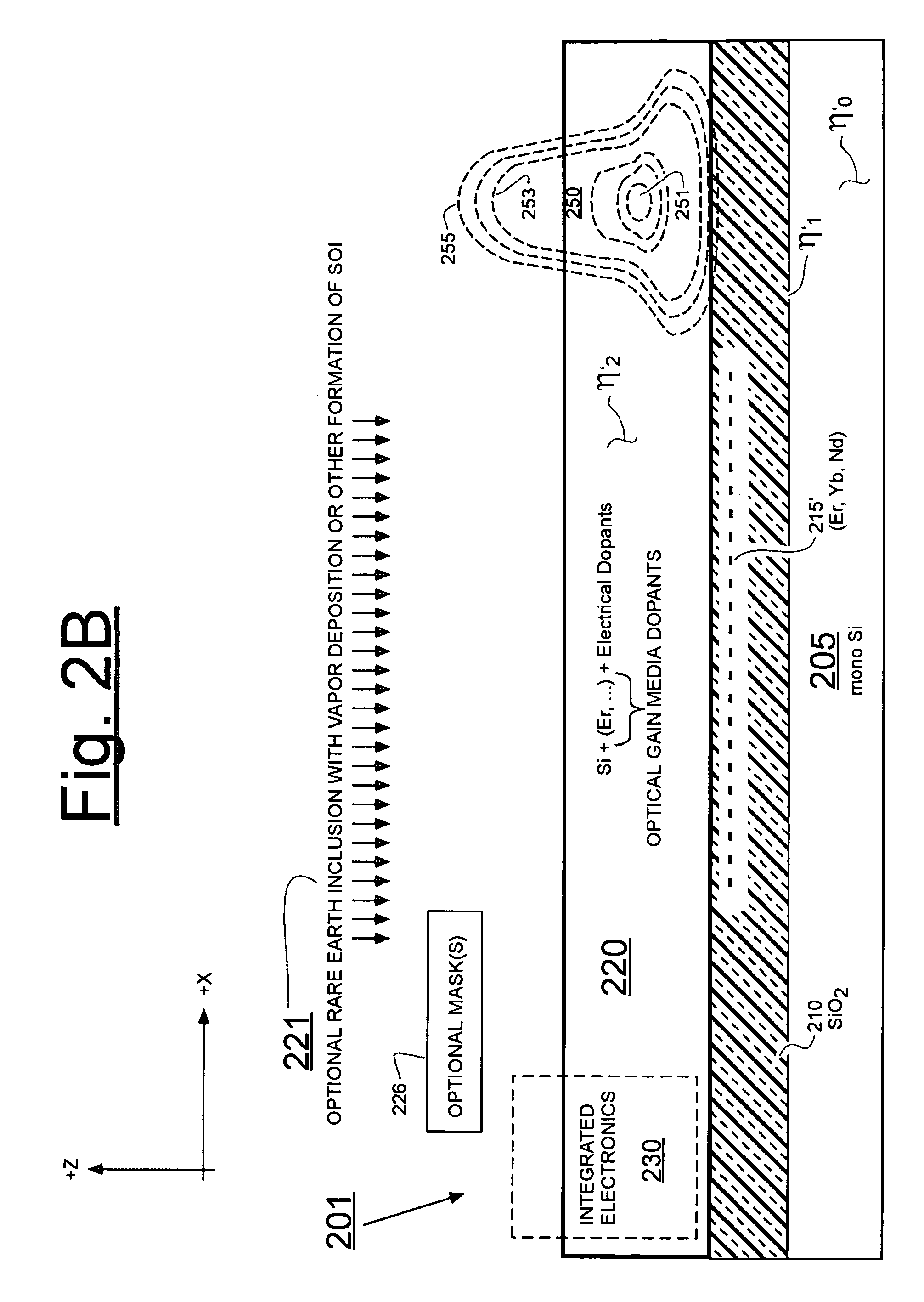
[0022] A method in accordance with the present disclosure for
mass producing integrated photonic and / or electro-photonic devices may include the steps of: (a) incorporating one or more rare earth elements with appropriate concentrations into
silicon and / or
silicon oxide and / or into other semiconductors and / or their
dielectric compounds, where the incorporation may occur as the semiconductor and / or semiconductor compound regions are being grown or otherwise formed directly on a monolithically integrated device or as they are formed for subsequent bonding to the monolithically integrated device and where the incorporation correspondingly defines one or more optical gain media regions within the integrated device; (b) defining respective signal input ports in the integrated device for receiving input optical signals into corresponding ones of the one or more optical gain media regions; (c) defining respective pump energy receiving means in the integrated device for receiving pump energy into corresponding ones of the one or more optical gain media regions; and (d) defining respective signal output means in the integrated device for outputting optical signals from corresponding ones of the one or more optical gain media regions. The fabrication process may further include the formation of appropriate pump energy guiding means for guiding radiative pump energy and / or injected
electrical current into the one or more optical gain media regions for promoting interaction between the pump energy, the input optical signal(s) and the incorporated, rare earth elements. The incorporation of the one or more rare earth elements may include the provision of one or more binding agents such as
oxygen for enhancing binding between the rare earth elements (e.g., Er) and the
host material (e.g., monocrystalline Si) and / or the provision of one or more
trapping layers (e.g., amorphous Si and / or
amorphous silicon oxide) so as to reduce out-
diffusion of the incorporated
rare earth element(s) and / or the provision of one or more rapid
thermal treatment steps so as to activate the incorporated
rare earth element(s) within their respective parts of the
host material.

