Semiconductor device and method of manufacturing the same

Inactive Publication Date: 2009-05-21
SHOWA DENKO KK +1
View PDF7 Cites 22 Cited by
  • Summary
  • Abstract
  • Description
  • Claims
  • Application Information

AI Technical Summary

Benefits of technology

[0042]Particularly, according to the present invention, a hydrocarbon gas is blown onto the surface of the substrate composed of a silicon single crystal and hydrocarbon is caused to be adsorbed onto the surface of the silicon single crystal substrate by radiating electrons onto the surface of the silicon single crystal substrate, whereby a cubic silicon carbide layer whose lattice constant exceeds 0.436 nm and is not more than 0.460 nm and which has a nonstoichiometric composition containing silicon abundantly in terms of composition is formed. Therefore, it is possible to stably form a silicon carbide layer that has especially few crystal defects and is excellent in crystallinity and hence it is possible to stably manufacture a high-performance semiconduc

Problems solved by technology

However, because sapphire, which is used as a material for the substrate of a Group III nitride semiconductor device, has electrical insulating properties, the material has for example the problem that it is not easy to obtain Group III nitride LEDs having high breakdown voltage properties against static electricity and the like.
However, because sapphire does not have high thermal conductivity, it has been difficult to fabricate field-effect transistors (hereinafter abbreviated as “FETs”) of low loss in which the heat radiating properties of a substrate are utilized.
However, a silicon carbide bulk single crystal having a diameter that is appropriately large for use in a substrate is expensive and this is unfavorable for the manufacture of consumer Group III nitride semiconductor devices.
Therefore, a large lattice mismatch exists between the two materials.
For this reason, a silicon single crystal has the disadvantage that it is difficult to stably form a superior-quality Group III nitride semiconductor layer having few crysta

Method used


Image

  • Semiconductor device and method of manufacturing the same
  • Semiconductor device and method of manufacturing the same
  • Semiconductor device and method of manufacturing the same

Examples


Example

EMBODIMENT 1

[0073]In Embodiment 1, the present invention will be described in detail by taking, as an example, a case where a light emitting diode (LED) is fabricated from an epitaxially stacked structure including a silicon carbide layer of a nonstoichiometric composition provided on a (111) silicon single crystal substrate whose surface is a (111) crystal plane, a hexagonal Group III nitride semiconductor junction layer, a superlattice-structured layer constituted by hexagonal Group III nitride semiconductor layers.

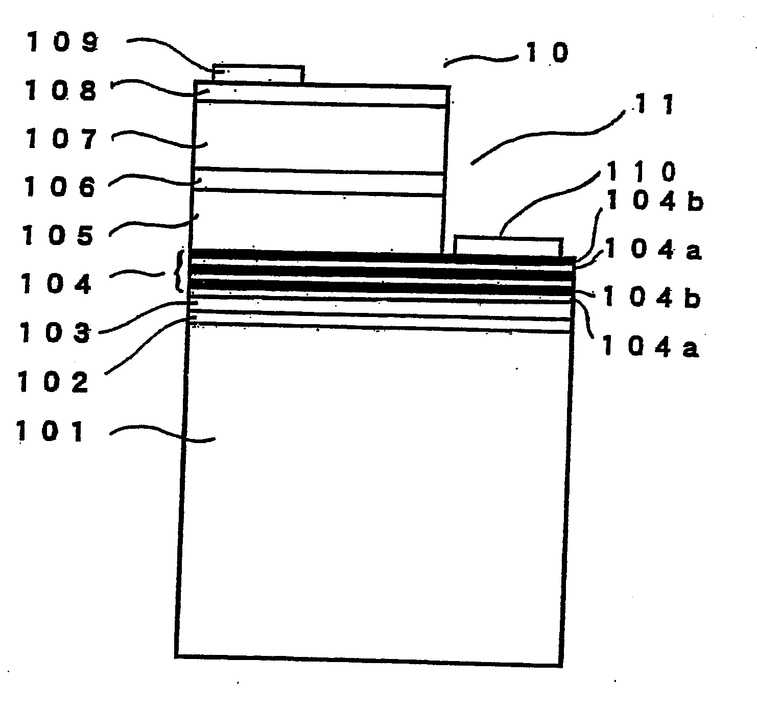
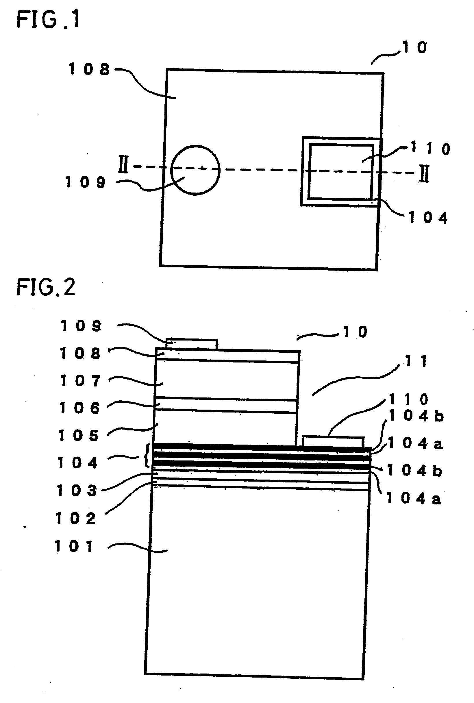
[0074]The plane structure of a semiconductor LED 10 fabricated in Embodiment 1 is schematically shown in FIG. 1. The sectional structure of the LED 10 of FIG. 10 taken along the broken line II-II is schematically shown in FIG. 2.

[0075]In the fabrication of the LED 10, a P type silicon single crystal having a (111) crystal plane as the surface, to which boron (element symbol: B) is added, was used as a substrate 101. After the substrate 101 was transported into a growth ...

Example

EMBODIMENT 2

[0084]In Embodiment 2, the present invention will be described in detail by taking, as an example, a case where a light emitting diode (LED) is fabricated from an epitaxially stacked structure including a silicon carbide layer of a nonstoichiometric composition provided on a (001) silicon single crystal substrate whose surface is a (001) crystal plane, a cubic Group III nitride semiconductor junction layer, a superlattice-structured layer constituted by cubic Group III nitride semiconductor layers.

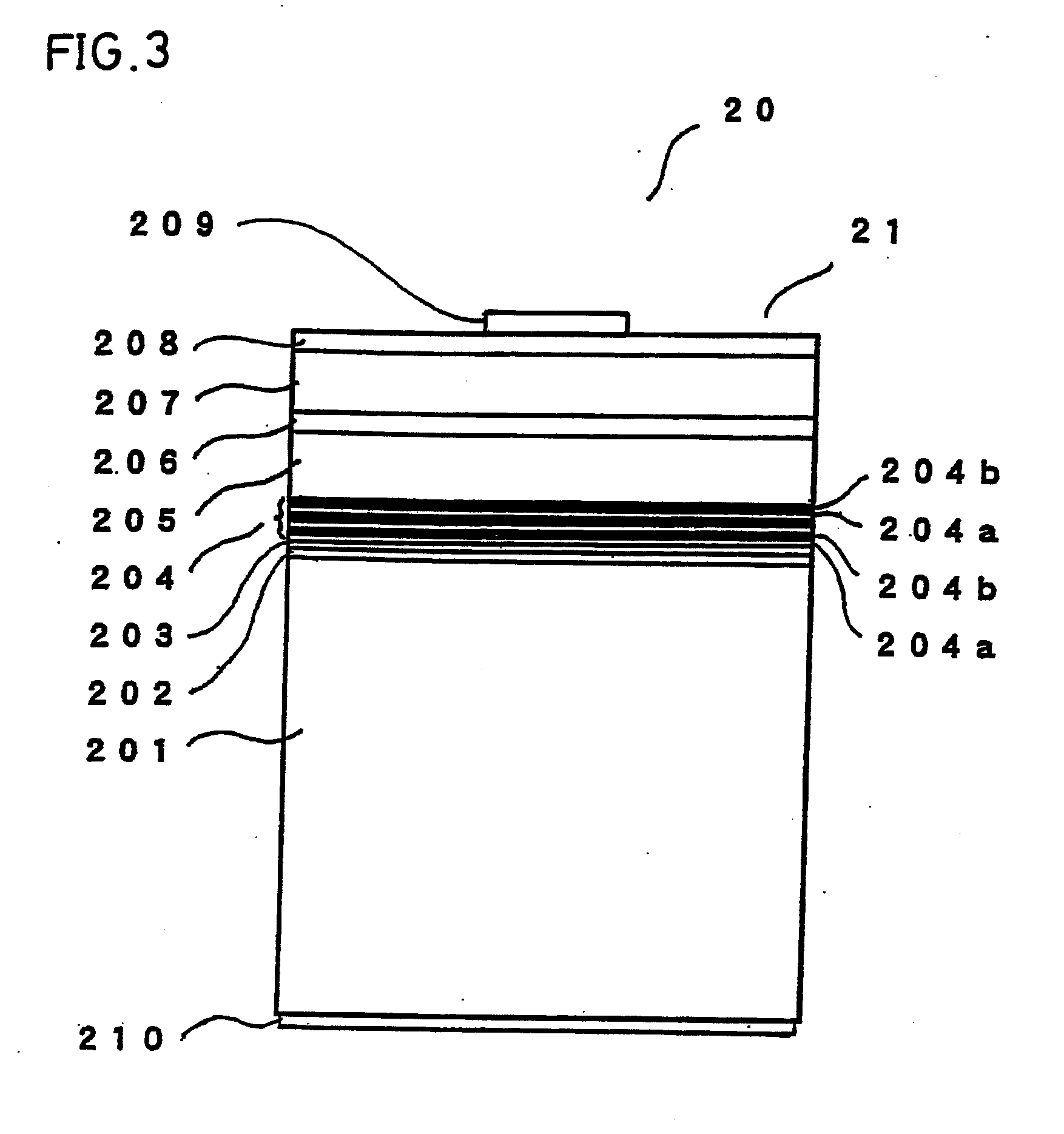
[0085]The planar structure of a semiconductor LED 10 fabricated in Embodiment 2 is schematically shown in FIG. 2.

[0086]In the fabrication of the LED 20, an N type silicon single crystal having a (001) crystal plane as the surface, to which phosphorus (element symbol: P) is added, was used as a substrate 201. After the substrate 201 was transported into a growth chamber for MBE growth, the substrate 201 was heated to 800° C. in a high vacuum of approximately 5×10⁻⁷ pascals (Pa)....

Example

EMBODIMENT 3

[0095]The present invention in this embodiment will be concretely described by taking, as an example, a case where an LED having a Group III nitride semiconductor junction layer composed of aluminum nitride formed by nitriding a metal aluminum film is fabricated.

[0096]As described in Embodiment 1 above, a cubic 3C-type silicon carbide layer was formed on a (111) silicon single crystal substrate whose surface is a (111) crystal plane. Next, within an MBE growth chamber, aluminum (Al) beams were radiated onto the surface formed from a (111) crystal plane of the silicon carbide layer having a lattice constant of 0.450 nm, whereby an Al film was formed. The film thickness of the Al film was set at approximately 3 nm.

[0097]Next, by use of an ECR (electron cyclotron resonance) type radio-frequency (RF) plasma generator provided in the MBE growth chamber, a nitrogen plasma was generated within the chamber. After that, nitrogen radicals in the nitrogen plasma were selectively ex...


PUM


Abstract

Provided is a semiconductor device containing a silicon single crystal substrate 101, a silicon carbide layer 102 provided on a surface of the substrate, a Group III nitride semiconductor junction layer 103 provided in contact with the silicon carbide layer, and a superlattice-structured layer 104 constituted by Group III nitride semiconductors on the Group III nitride semiconductor junction layer. In this semiconductor device, the silicon carbide layer is a layer of a cubic system whose lattice constant exceeds 0.436 nm and is not more than 0.460 nm and which has a nonstoichiometric composition containing silicon abundantly in terms of composition, and the Group III nitride semiconductor junction layer has a composition of AlxGayInzN1-αMα (0≦X, Y, Z≦1, X+Y+Z=1, 0≦α<1, M is a Group V element except nitrogen).

Description

TECHNICAL FIELD OF[0001]The present invention relates to a semiconductor device formed from a stacked structure having a substrate of a silicon single crystal and a Group III nitride semiconductor layer.BACKGROUND ART[0002]Gallium nitride (GaN) and aluminum nitride (AlN) have (hitherto) been known as Group III nitride semiconductors. These Group III nitride semiconductor materials are used to form semiconductor light emitting devices, such as light emitting diodes (hereinafter abbreviated as “LEDs”), which emit blue, green or otherwise visible light of short wavelength, and laser diodes (hereinafter abbreviated as “LDs”) (refer to, for example, JP-A SHO 54-3834 (Patent Document 1)). Also, these Group III nitride semiconductor materials are used to form electronic devices such as high-frequency transistors (refer to, for example, M. A. Kahn et al., Applied Physics Letters (Appl. Phys. Lett.), USA, 1993, Vol. 62, p. 1786 (Non-patent Document 1)).[0003]In such semiconductor devices com...

Claims


Application Information

Patent Timeline
IPC IPC(8): H01L29/267H01L21/205H01L33/06H01L33/16H01L33/32H01L33/34
CPCB82Y20/00C30B29/36H01L2924/0002C30B29/40C30B29/403C30B29/68H01L21/02381H01L21/02433H01L21/02447H01L21/02516H01L21/02538H01L21/0254H01L21/0262H01L33/007H01L33/04H01L33/12H01S5/021H01S5/32341H01S5/34333H01L2924/00
Inventor OHACHI, TADASHIUDAGAWA, TAKASHI
Owner SHOWA DENKO KK
Why Eureka
Try Eureka