[0035]The present invention is directed to a photo detection device, which can solve or alleviate the problems that the before-mentioned conventional devices have. The device can greatly suppress the
noise generation resulting from
dark current, especially in an HPT for detecting the middle-infrared spectral range and has a high sensitivity and furthermore an extensive
wavelength band characteristics. Therefore, in general terms, the optimization of a
transistor region and a
photodiode region is performed using the device structure designing and the
band gap engineering technique. That is, the
optimal design of the energy profile of a conduction band and a
valence band is carried out independently, and while transporting smoothly the photo carriers generated in a
photodiode region to a
transistor region, generation of the leakage current in
peripheral is controlled.
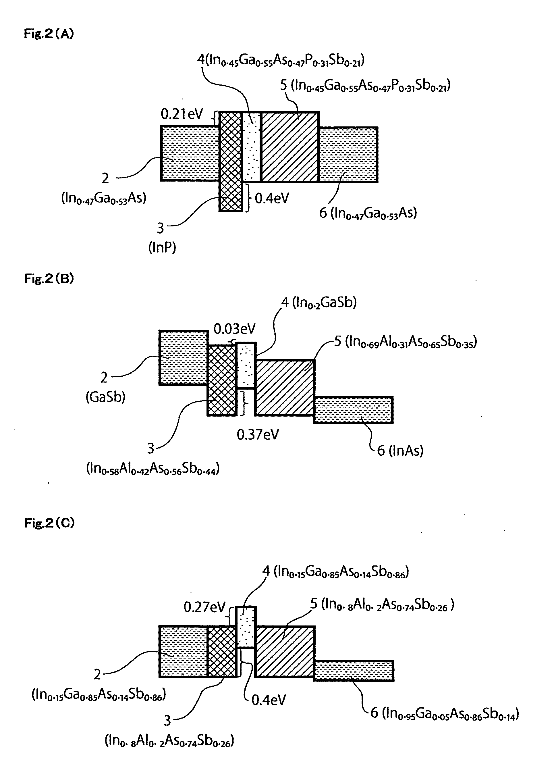
[0046]Furthermore, even if a photo-absorption layer is composed of a
narrowband-gap material, hole injection to a barrier layer from a photo-absorption layer under no
light irradiation can be suppressed, for example, by making a photo-absorption layer n type and lowering the hole concentration in a
thermal equilibrium state. On the other hand, the
electron current generated in a collector operating as the barrier layer is suppressed because the collector operating as the barrier layer comprises a
wideband gap semiconductor and the
electron concentration in a
thermal equilibrium state can be set low. In addition, the
electric field in a photo-absorption layer is eased as much as the difference between the energy level in the conduction band of a photo-absorption layer and that of a collector operating as a barrier layer so that the generation of electron-hole pairs in a
depletion region under no
light irradiation is suppressed.
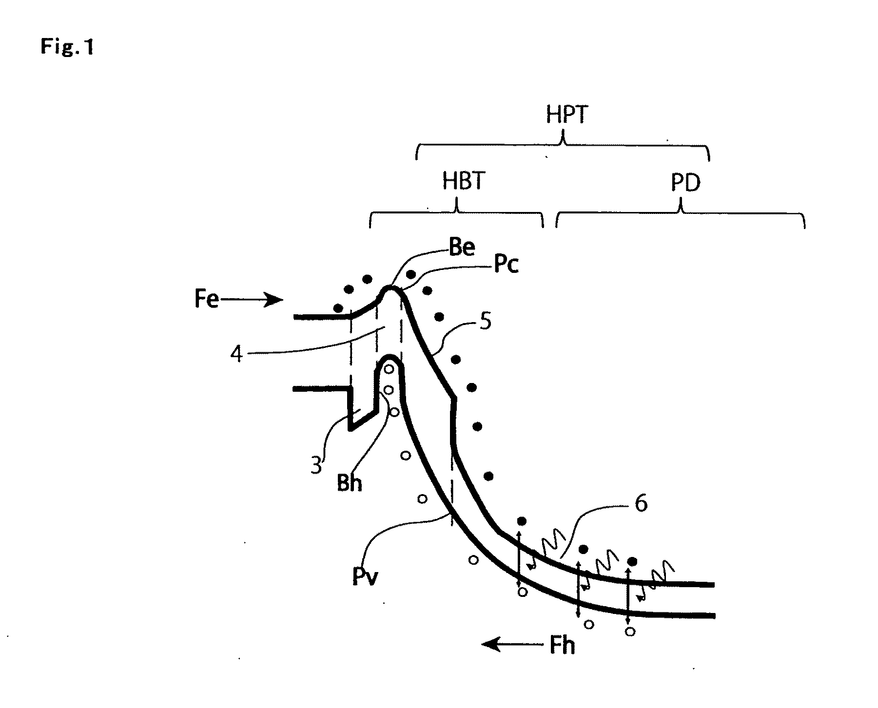
[0047]According to the present embodiment, if the junction of a collector operating as a barrier layer, and a photo-absorption layer becomes a Type 2
heterojunction, a potential slope from a collector operating as the barrier layer to a photo-absorption layer can be formed without a barrier as to electrons, and a potential slope from a photo-absorption layer to a collector or the barrier layer can be formed without a barrier as to holes, that is, a barrier-free structure can be formed in a conduction band and a valence band respectively. Electrons and holes flow in opposite directions and also they are separated to some extent in the planar configuration. Therefore, in an HPT of the present embodiment, an
optimal design for each independent view is possible such as in terms of amplification rate, a base layer and an emitter layer as an
electron device, and in terms of
quantum efficiency, a photo-absorption layer and a collector operating as a barrier layer as a photodiode.
[0049]In the conventional
transistor amplifying circuits, it is common to wire a proper
resistor between an emitter base and a base or a collector, and to design bias current and
gain levels. However, in the case of HPT aiming at the very weak
photodetection of pW level, the range of the optimal
resistor will need to be set to G
ohm and may need to use special high
resistor and circuit board. However, according to the present embodiment, it becomes possible to set up the bias conditions freely, and implementation to a device becomes easy as a two-terminal device by designing the potential of the conduction band of a base layer in the case of an open base HPT.
[0050]Generally, the surface defect density of a
crystal is larger than the inside of a
crystal, and the carrier recombination and the generation effects in
crystal defective levels are proportional to an equilibrium carrier concentration. Therefore, in order to prevent the decrease of the transistor current gain caused by carrier recombination and increase of dark current by carrier generation, it is effective to form a pn junction exposed at the surface composed of a
wideband gap semiconductor only, and to maintain its
thermal equilibrium conditions as unique
conductivity on a
narrow band gap surface. The specific embodiment of the present embodiment also realizes such a dark current suppression mechanism.
[0051]An HPT of this present embodiment where a phototransistor elements is optimally designed by the arts of the
band gap engineering and surface treatment becomes a wide range middle-infrared
photodetection device with much higher sensitivity even under
operating environment near
room temperature and making dark current lower less than one tenth and amplification rate higher compared to the conventional middle-infrared photo detection device.

