Very high transmittance, back-illuminated, silicon-on-sapphire semiconductor wafer substrate for high quantum efficiency and high resolution, solid-state, imaging focal plane arrays

a semiconductor wafer and quantum efficiency technology, applied in the field of very high transmittance, back illumination, silicon-on-sapphire semiconductor wafer substrates for high quantum efficiency and high resolution, solid-state imaging focal plane arrays, etc., can solve problems such as refractive index mismatch, and achieve high transmittance, high transmittance, and high transmittance. high

Inactive Publication Date: 2012-08-02
STERN ALVIN GABRIEL
View PDF4 Cites 26 Cited by
  • Summary
  • Abstract
  • Description
  • Claims
  • Application Information

AI Technical Summary

Benefits of technology

[0022]The very high transmittance, back-illuminated silicon-(AlN / a-SiNX<1.33)-sapphire substrate with λ / 4-MgF2 back-side antireflective layer, readily supports fabrication of silicon mesa detectors with exposed (111) side planes and fixed crystallographic angle φC=54.7° between (100) and (111) silicon planes, by liquid anisotropic etching using tetramethyl ammonium hydroxide (TMAH) to define the APD detector array. The AlN / a-SiNX<1.33 antireflective bilayer and sapphire act as natural etch stopping layers to enable fabrication of highly uniform silicon mesa pixels by crystallographic etching. In addition, monolithic sapphire microlenses can be fabricated beneath each mesa APD detector pixel in the thinned sapphire to focus light under the full height of the detector mesas. The space between mesa APD detector pixels can be filled by an aluminum (Al) or copper (Cu) metal anode grid, forming a common anode electrical connection at the base of each silicon detector mesa. The Al metal common anode grid also performs the important secondary function of providing optical crosstalk isolation between adjacent APD detectors by blocking light emitted during the avalanche gain process.
[0023]The design of the very high transmittance, back-illuminated silicon-(AlN / a-SiNX<1.33)-sapphire substrates allows the complete substrate to be fabricated prior to the fabrication of Si or SiGe APD detectors in the silicon device layer, since none of the material layers in the substrate including AlN, a-SiNX<1.33 and sapphire will be adversely affected by subsequent APD detector device fabrication in the silicon mesas using conventional silicon processing technology (e.g. thermal oxidation, diffusion of dopant impurities, deposition and metallization steps). If required, the λ / 4-MgF2 back-side antireflective layer can be protected by depositing an SiO2 cladding layer prior to the APD detector array fabrication, that can be etched off using liquid HF once the detector processing has been completed. Being able to fully fabricate and characterize the very high transmittance, back-illuminated silicon-(AlN / a-SiNX<1.33)-sapphire substrates with back-side λ / 4-MgF2 antireflective layer prior to fabricating the silicon detectors is cost effective, first, by allowing wafer substrates to be optimally fabricated, separately and independently from the detector devices, and second, by preventing the consumption of expensive semiconductor gases to manufacture detectors in unfinished wafer substrates that might not pass quality standards once fully fabricated.
[0024]In summary, an optimized silicon-(AlN / a-SiNX<1.33)-sapphire substrate with back-side λ / 4-MgF2 antireflective layer, having a properly designed thickness of AlN and MgF2 layers as well as properly designed thickness and composition of a-SiNX<1.33, can achieve nearly 100% back-illuminated optical transmittance over a broad wavelength range from 250-1100 nm. The very high transmittance substrate will support the fabrication of high quantum efficiency and high resolution, back-illuminated silicon and silicon-germanium APD detector arrays with effective optical crosstalk isolation between neighboring pixels in the array. The silicon-(AlN / a-SiNX<1.33)-sapphire substrate with back-side λ / 4-MgF2 antireflective layer can be fabricated separately and independently from the detector device arrays. Thus, there is no need to potentially waste expensive resources to manufacture detector arrays in unfinished wafer substrates that might not pass quality standards once fully fabricated.

Problems solved by technology

The main problem of transmitting broadband light through the transparent sapphire substrate into the silicon detector device layer in conventional silicon-on-sapphire wafer substrates, occurs due to the optical reflection losses at the sapphire-silicon and the air-sapphire material interfaces, resulting from refractive index mismatch between the layers.

Method used


Image

  • Very high transmittance, back-illuminated, silicon-on-sapphire semiconductor wafer substrate for high quantum efficiency and high resolution, solid-state, imaging focal plane arrays
  • Very high transmittance, back-illuminated, silicon-on-sapphire semiconductor wafer substrate for high quantum efficiency and high resolution, solid-state, imaging focal plane arrays
  • Very high transmittance, back-illuminated, silicon-on-sapphire semiconductor wafer substrate for high quantum efficiency and high resolution, solid-state, imaging focal plane arrays

Examples


Embodiment Construction

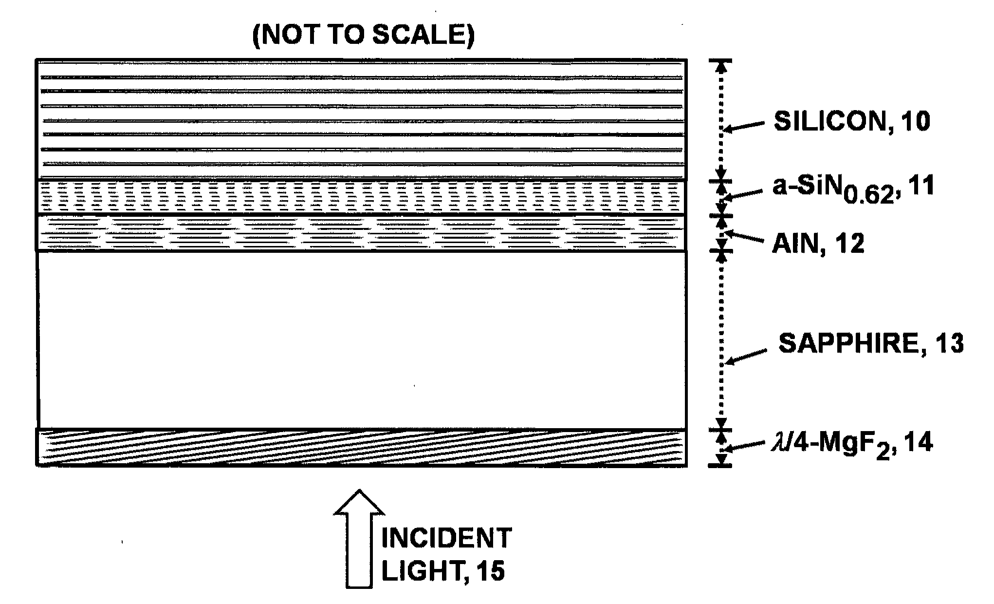
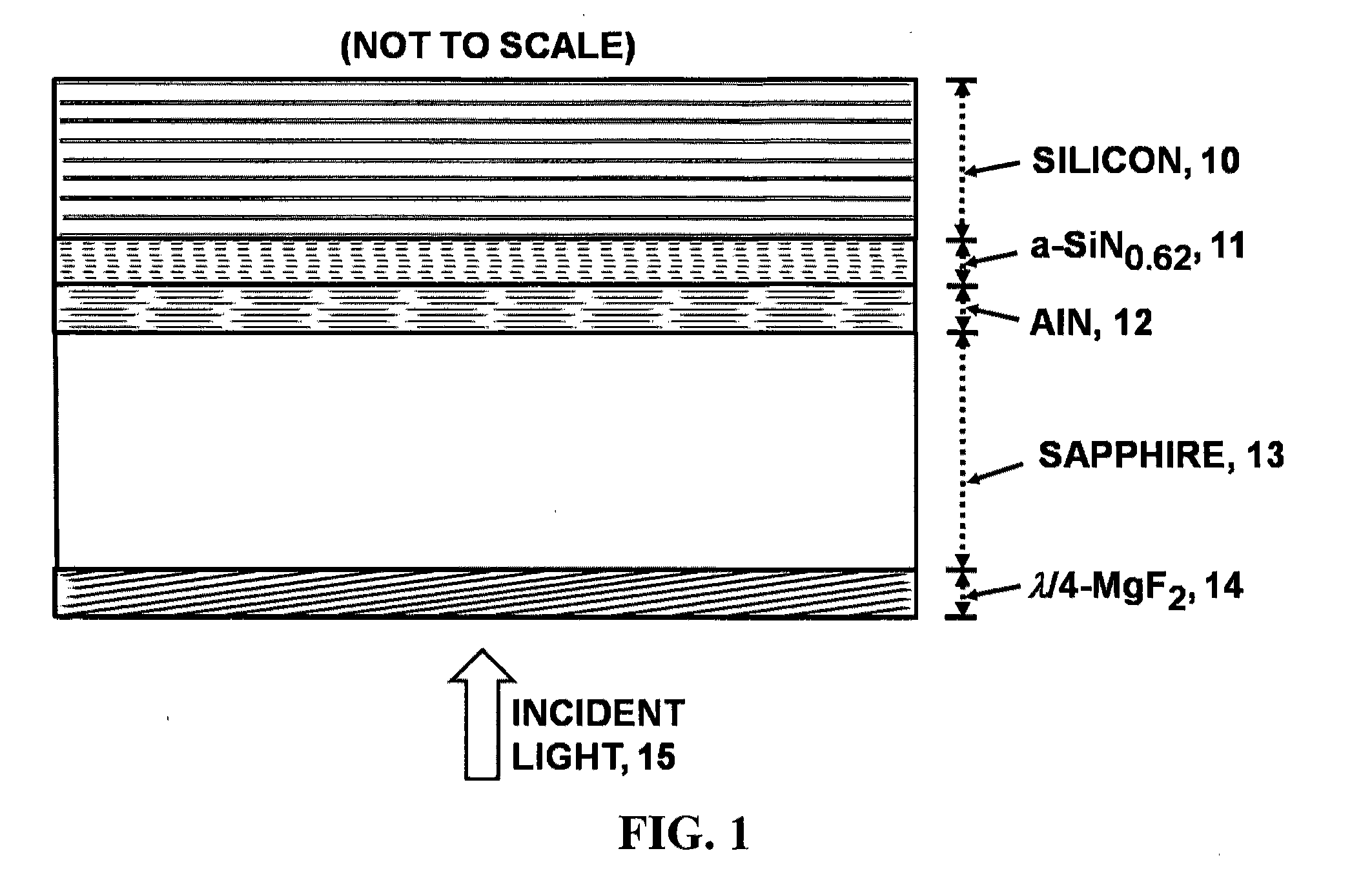
[0033]Referring to FIG. 1, a depiction of the very high transmittance, back-illuminated, silicon-on-sapphire semiconductor wafer substrate is shown in a non-scale rendering, consisting of an ordered stacking of material layers including the top most single crystal silicon (Si) semiconductor layer 10, non-stoichiometric, silicon rich, amorphous silicon nitride antireflective layer with nitrogen to silicon ratio N:Si=0.62 or a-SiN0.62 11, single crystal aluminum nitride (AlN) antireflective layer 12, optically transparent single crystal sapphire (α-Al2O3) wafer substrate 13, and back-side one quarter wavelength thick magnesium fluoride (λ / 4-MgF2) antireflective layer 14. Solid-state detector devices are meant to be fabricated in the silicon 10 semiconductor layer and back-illuminated by light 15 incident from the back-side of the substrate that traverses the optimal thickness material layers λ / 4-MgF2, sapphire, AlN and a-SiN0.62 with minimal reflection and absorption losses, to enter ...


PUM


Abstract

An advanced, very high transmittance, back-illuminated, silicon-on-sapphire wafer substrate design is presented for enabling high quantum efficiency and high resolution, silicon or silicon-germanium avalanche photodiode detector arrays. The wafer substrate incorporates a stacked antireflective bilayer between the sapphire and silicon layers, comprised of single crystal aluminum nitride (AlN) and non-stoichiometric, silicon rich, amorphous silicon nitride (a-SiNX<1.33), that provides optimal refractive index matching between sapphire and silicon. A one quarter wavelength, magnesium fluoride (λ/4-MgF2) antireflective layer deposited on the back surface of the thinned sapphire provides refractive index matching at the air-sapphire interface. Selecting a composition of x=0.62 for a-SiNX, tunes an optimal refractive index for the layer. Selecting design thicknesses of 52 nm for single crystal AlN, 30 nm for a-SiN0.62, and 120 nm for λ/4-MgF2 yields a back-illuminated optical transmittance T>50% for 250-300 nm, T>70% for 300-400 nm and T>90% for 400-1100 nm.

Description

CROSS-REFERENCE TO RELATED APPLICATIONS[0001]Not ApplicableSTATEMENT REGARDING FEDERALLY SPONSORED RESEARCH OR DEVELOPMENT[0002]Not ApplicableREFERENCE TO SEQUENCE LISTING, A TABLE, OR A COMPUTER PROGRAM LISTING COMPACT DISC APPENDIX[0003]Not ApplicableBACKGROUND OF THE INVENTION[0004]For the purposes of imaging a scene, at low ambient illumination levels using a focal plane array comprised of solid-state detector devices, it is beneficial for the individual detectors in the array to be sensitive to light over a broad wavelength range and at single photon intensity levels. To support the fabrication of such an array of highly sensitive solid-state light detectors over broad spectral range, the back-illuminated semiconductor wafer substrate on which the detector devices are fabricated should be capable of transmitting light into the detectors with high efficiency from the ultraviolet to the midwave infrared for enabling high quantum efficiency detectors. The back-illumination approac...

Claims


Application Information

Patent Timeline
Patent Type & Authority Applications(United States)
IPC IPC(8): H01L29/20H01L21/205
CPCH01L27/1464H01L31/1075H01L31/02165
Inventor STERN, ALVIN GABRIEL
Owner STERN ALVIN GABRIEL
Why Eureka
Try Eureka