Unlock instant, AI-driven research and patent intelligence for your innovation.
Manufacturing method for electronic device
Active Publication Date: 2020-08-20
KONICA MINOLTA INC
View PDF0 Cites 0 Cited by
Summary
Abstract
Description
Claims
Application Information
AI Technical Summary
This helps you quickly interpret patents by identifying the three key elements:
Problems solved by technology
Method used
Benefits of technology
Benefits of technology
The present invention provides a method for manufacturing an electronic device with an organic thin film functioning as a sealing film against moisture permeation for an electronic device such as an organic electroluminescent element. The sealing film releases a hydrophobic substance by an amount corresponding to the reaction with water (moisture) and prevents further penetration of water. The method involves using a new desiccant and an organic thin film containing the desiccant, which exhibits a synergistic effect in preventing moisture penetration. The organic thin film containing the desiccant can be formed using a sol-gel method.
Problems solved by technology
The manufacturing method (1) is characterized in that it is manufactured by vacuum deposition typified by vapor deposition, sputtering, CVD (Chemical Vapor Deposition), and ALD (Atomic Layer Deposition), and is excellent in water vapor barrier property because a plurality of dense films can be formed, but on the other hand, the manufacturing method requires a large-sized device and is unsuitable for continuous production such as roll-to-roll, so that the manufacturing cost is high and the problem is large for mass and inexpensive production.
On the other hand, the method for removing the water molecules of (2) and (3) can be selectively used depending on the allowable moisture concentration of the device, but in general, the desorption phenomenon of water molecules cannot be avoided if the adsorption mechanism is the chemical equilibrium between water and adsorbent, such as silica gel, zeolite, montmorillonite of (2), and the method cannot be applied to organic thin film solar cells or organic EL elements that require a high degree of water molecule removal.
The method (3) typified by bariumoxide, or strontiumoxide has excellent ability as a desiccant because it has high reactivity with water molecules, but has many problems such as immediate reaction with water at atmospheric pressure, deterioration in performance, and the attendant risk of heat generation, and the effect is temporary and unsuitable for long-term storage because only stoichiometric amounts of water can be captured in the device.
However, the disclosed alumina ring trimer still has a low water vapor barrier property for application to a sealing film of an electronic device.
Method used
Image
Click on the blue label to locate the original text in one second.
Reading with bidirectional positioning of images and text.
Examples
example 1
(Preparation of Organic EL Element)
[0317]A glass substrate on which a 100 nm-thick film of ITO (IndiumTinOxide) was formed as an anode was subjected to ultrasonic cleaning with isopropylalcohol, dried with dry nitrogen gas and UV-ozone cleaning, and fixed to a substrate holder of a vacuum evaporation device.
[0318]Then, HAT-CN (1,4,5,8,9,12-hexaazatriphenylene hexacarbonitrile) was evaporated to a thickness of 10 nm to provide hole injection-transport layer.
[0320]Then, mCP (1,3-bis(N-carbazolyl)benzene) as a host material and bis[2-(4,6-difluorophenyl)pyridinato-C2,N)(picolinato)iridium(III)(FIrpic) as a light-emitting compound were co-evaporated to be 94% and 6% by volume, respectively, to provide a 30 nm-thick light-emitting layer.
[0321]Thereafter, BCP (2,9-dimethyl-4,7-diphenyl-1,10-phenanthroline) was v...
example 2
[0341]Using the same constitution as that of the sealing film 1 of Example 1, the metalalkoxide and the metalcarboxylateraw material used for the sealing film were changed as indicated in Table II, and the sealing performance was evaluated.
[0342]The composition and evaluation results of the sealing film are indicated in Table II.
[0344]The sol-gel solution used in Example 1 was applied onto a siliconwafer, and a thin film was produced under the same film forming conditions as in Example 1. The prepared thin film was analyzed by the above-mentioned SEM / EDS (Energy Dispersive X-ray Spectoroscopy: energy-dispersive X-ray analyzer) to obtain the values of the following expression (a). SEM / EDS equipment was made by JSM-IT100 (JEOL Ltd).
[0345]Elemental analysis by SEM / EDS (energy dispersive X-rayspectrometer) and the values obtained by the following expression (a) are indicated in Table III.
F / (C+F) Expression (a):
(In Expression (a), F and C represent the concentrations of fluorine and carbon atoms, respectively.)
[0346]From the results in Table III, it was confirmed that the thin film prepared from the sol-gel solution of Example 1 retained fluorine atoms in the film at a ce...
PUM
Abstract
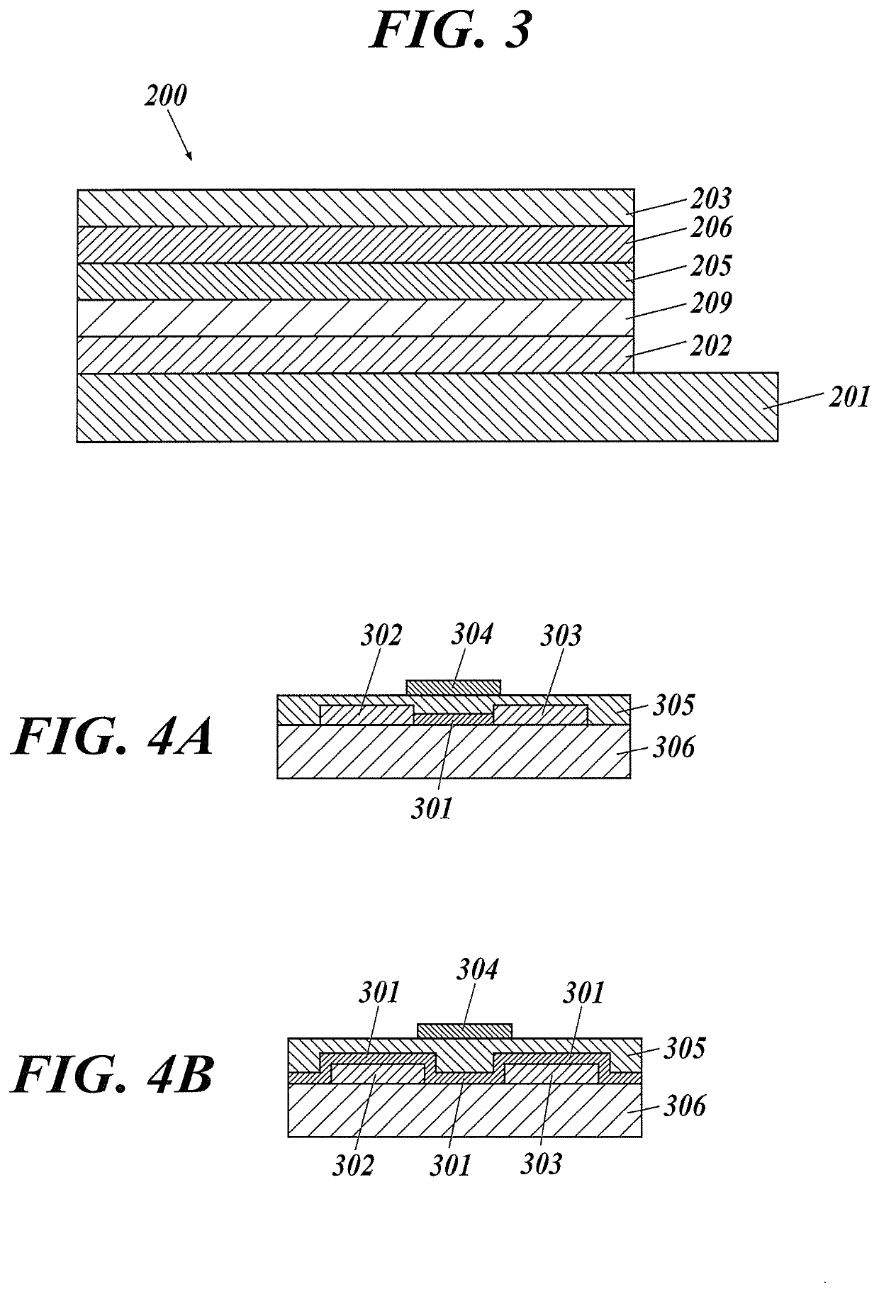
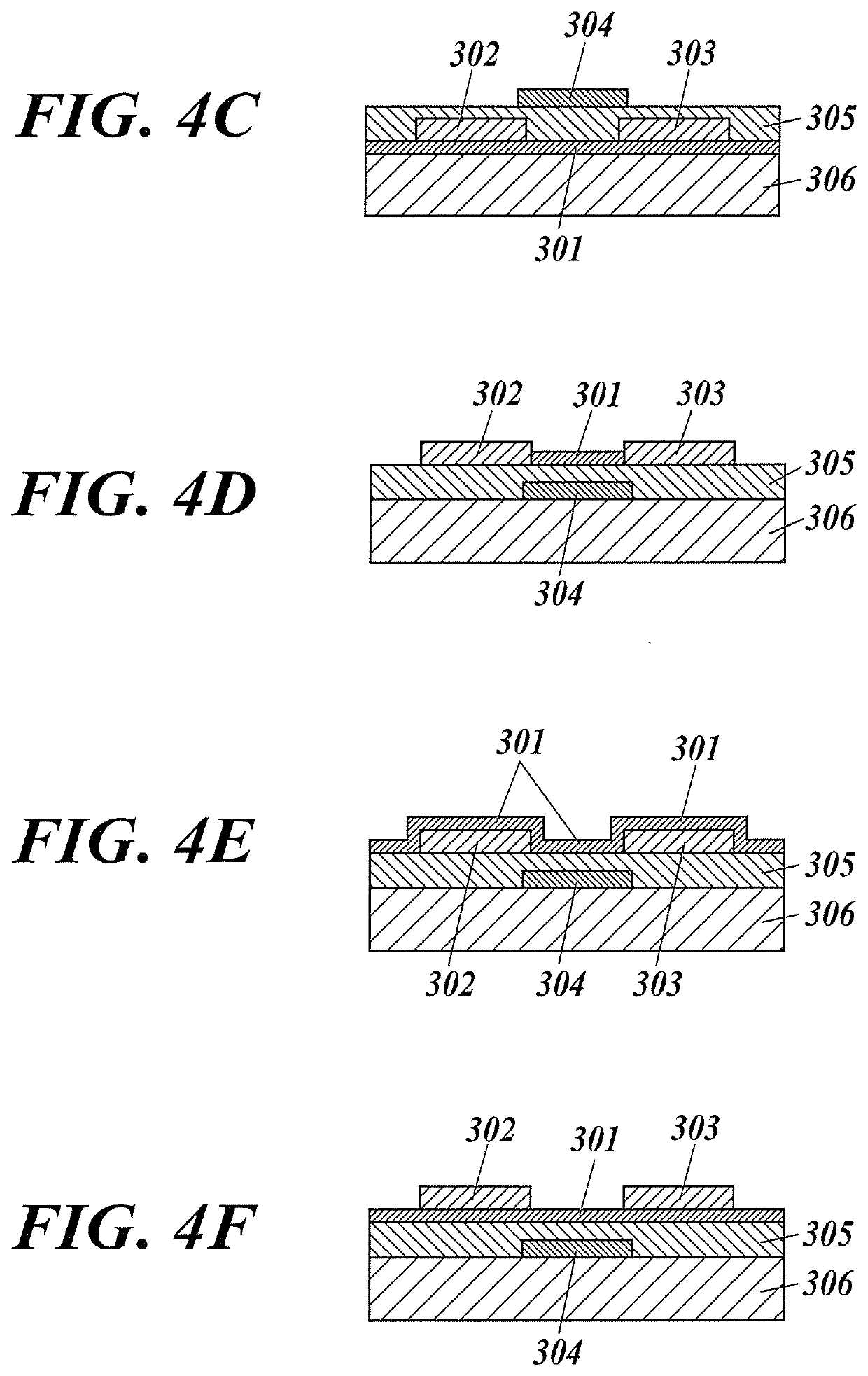
The present invention addresses the problem of providing a manufacturing method for an electronic device that is provided with an organic thin film functioning as a sealing film against moisturepermeation in an electronic device such as an organic electroluminescence element. This manufacturing method for an electronic device is a manufacturing method for an electronic device that has at least an organic functional layer, an elution prevention film, and a sealing film in this order, said manufacturing method being characterized by having: a step in which, after coating is performed with a silicone resin, the result is irradiated with vacuum ultraviolet rays to form the elution prevention film; and a step in which, after the elution prevention film is coated with a liquid mixture of a metalalkoxide and a fluoroalcohol, the result is irradiated with vacuum ultraviolet rays to form the ultraviolet rays to form the sealing film.
Description
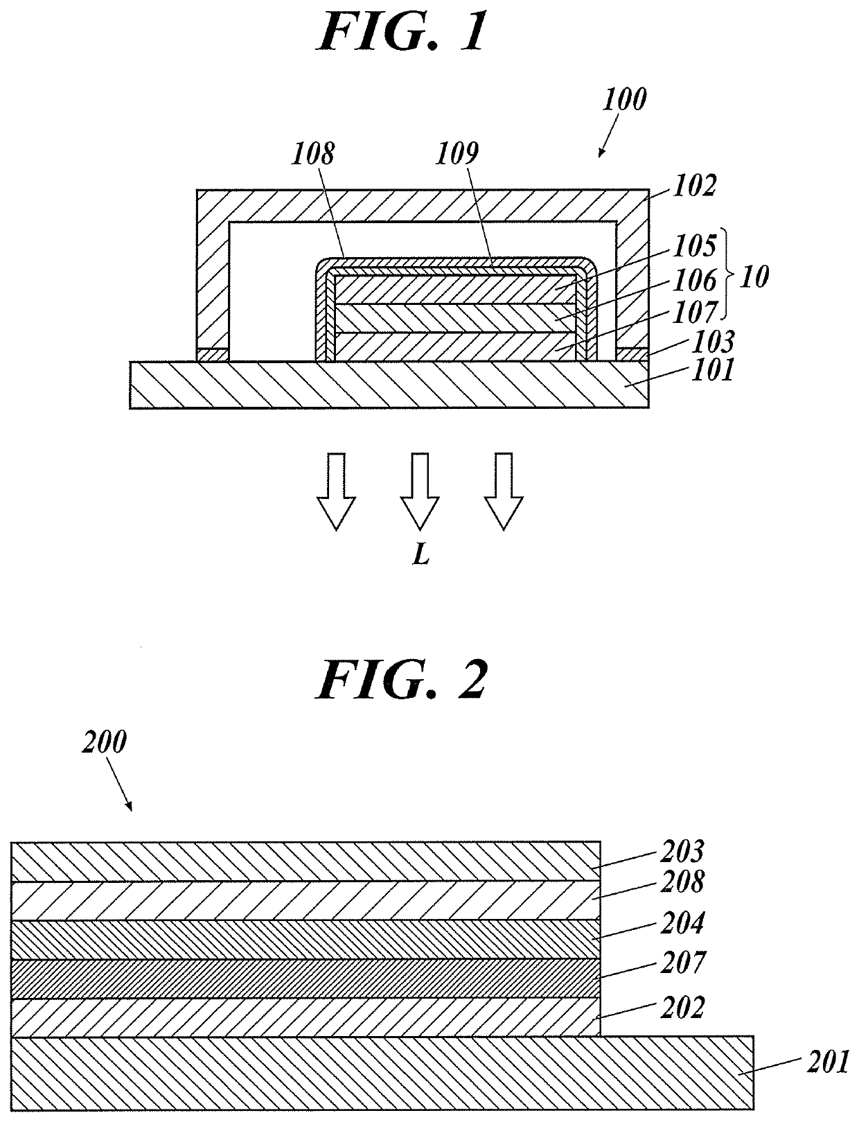
TECHNICAL FIELD[0001]The present invention relates to a method of manufacturing an electronic device, and more particularly, the present invention relates to a method of manufacturing an electronic device comprising an organic thin film functioning as a moisture permeable sealing film for an electronic device such as an organic electroluminescent element.BACKGROUND[0002]In the industry, a number of electronic components, including transistors and diodes, are subjected to a process called sealing (passivation) to avoid the degradation caused by water and oxygen. In particular, organic thin film transistors, organic thin film solar cells, and organic electroluminescence elements (hereinafter referred to as organic EL elements), in which electron conduction is performed by organic compounds, are particularly sensitive to water molecules, and extremely high sealing is required. Among them, since the organic EL element is in an excited state having the highest reactivity as an organic ma...
Claims
Application Information
Patent Timeline
Application Date:The date an application was filed.
Publication Date:The date a patent or application was officially published.
First Publication Date:The earliest publication date of a patent with the same application number.
Issue Date:Publication date of the patent grant document.
PCT Entry Date:The Entry date of PCT National Phase.
Estimated Expiry Date:The statutory expiry date of a patent right according to the Patent Law, and it is the longest term of protection that the patent right can achieve without the termination of the patent right due to other reasons(Term extension factor has been taken into account ).
Invalid Date:Actual expiry date is based on effective date or publication date of legal transaction data of invalid patent.

