Process for producing semiconductor article

Inactive Publication Date: 2003-03-18
CANON KK
View PDF31 Cites 424 Cited by
  • Summary
  • Abstract
  • Description
  • Claims
  • Application Information

AI Technical Summary

Benefits of technology

6. The possibility of producing fully depleted field effect transistors using the thin film technology. The advantages of the SOI technology are thoroughly discussed in Special Issue: "Single-crystal silicon on non-single-crystal insulators"; edited by G. W. Cullen, Journal of Crystal Growth, volume 63, No. 3, pp. 429-590 (1983).
In recent years, a number of reports have been published on the SOI technology for providing substrates that can realize high speed operation and low power consumption for MOSFETs (IEEE SOI conference 1994). The process of manufacturing a semiconductor device can be significantly enhanced by using the SOI structure when compared with the corresponding process of manufacturing a device on a bulk Si wafer, because of the implementation of a very simplified device isolation step. Thus, the use of the SOI technology can provide a significant cost reduction in manufacturing a semiconductor device, particularly in terms of the wafer cost and the process cost if viewed from the conventional technology of manufacturing a MOSFET or an IC on a bulk Si substrate, to say nothing of the remarkable performance of such a semiconductor device.
Fully depleted MOSFETs are very promising for achieving high speed operation and low power consumption if provided with improved drive power. Generally speaking, the threshold voltage (Vth) of a MOSFET is determined as a function of the impurity concentration of its channel section but, in the case of a fully depleted (FD) MOSFET, the characteristics of the depletion layer are influenced by the SOI film thickness. Theref

Problems solved by technology

However, a compound semiconductor substrate is costly and mechanically not very strong so that it is not adapted to produce a large wafer.
This technique is, however, accompanied by a problem that the isolated Si region is defined before the devices are produced and restricts the freedom of device design.
However, the allowable range of energy infusion and that of ion implantation are limited if the film quality of the Si oxide layer and the crystallinity of the surface Si layer are to be held to respective desired level.
Such a process by turn gives rise to a problem of uneven film thickness due to the intrinsic adverse effect of the process.
The SIMOX technique involves the use of a large volume of ions that is by far greater than the volume used in the ordinary semiconductor process and hence the ion implantation process may take a long time if a specifically designed apparatus is used for it.
Since the ion implantation process is performed typically by raster scanning of an ion beam showing a predetermined flow rate of electric current or by spreading an ion beam, a long time may be required for processing a large wafer.
Additionally, when a large wafer is processed at high temperature, the slip problem due to an uneven temperature distribution within the wafer can become very serious.
Since the SIMOX process requires the use of extraordinary high temperature that is as high as 1,320.degree. C., which is not observed in the ordinary Si semiconductor process, the problem of uneven temperature distribution will become more serious if a large wafer has to be prepared, unless a highly effective apparatus is not realized.
It is difficult to achieve an even film thickness by means of the polishing technique above.
Particularly, the mean deviation in the film thickness can be as large as tens of several percent to make the technique unfeasible when the film is thinned to an order of sub-micrometer.
This problem will become more significant for wafers having a large diameter.
However, this process is accompanied by a drawback that, if foreign objects are present on the substrate in the form of particles during the plasma etching, they operate as so many etching masks to produce projections on the substrate when the etching operation is over.
Then, again the problem of deviations in the film thickness due to polishing arises.
While the selective etching technique is effective for producing a thin film with an even film thickness, it is accompanied by the drawbacks as identified below.
The selective etching ratio is not satisfactory and will be as low as 10.sup.2 at most.
Therefore, the film thickness can lose the uniformity as it is reduced by polishing.
Particularly, while the polishing operation is controlled by the duration of the operation, it is difficult to rigorously control the operation because the polishing rate can vary significantly from time to time.
Thus, this problem becomes significant when forming an extremely thin SOI layer that is as thin as 100 nm.
The resulting SOI layer can show a poor crystallinity due to the use of a film forming technique that involve ion implantation and epitaxial or hetero-epitaxial growth on a Si layer that is densely doped with B. Additionally, the bonded surface of the substrate may show a degree of smoothness that is inferior relative to that of

Method used


Image

  • Process for producing semiconductor article
  • Process for producing semiconductor article
  • Process for producing semiconductor article

Examples


example 2

The surface layer of a monocrystalline Si wafer substrate was anodized in HF solution, under the following conditions:

current density: 7 (mA / cm.sup.2)

anodizing bath: HF:H.sub.2 O:C.sub.2 H.sub.5 OH=1:1:1

time: 11 minutes

porous Si thickness: 12 .mu.m

Then the substrate was oxidized for 1 hour at 400.degree. C. in oxygen atmosphere, whereby the internal wall of pores in the resulting porous Si layer was covered with a thermal oxidation film. Then, on the porous Si, monocrystalline Si was epitaxially grown, with a thickness of 0.15 .mu.m, by CVD (chemical vapor deposition) under the following conditions:

source gas: SiH.sub.2 Cl.sub.2 / H.sub.2

gas flow rate: 0.5 / 180 l / min.

gas pressure: 80 Torr

temperature: 950.degree. C.

growth rate: 0.3 .mu.m / min.

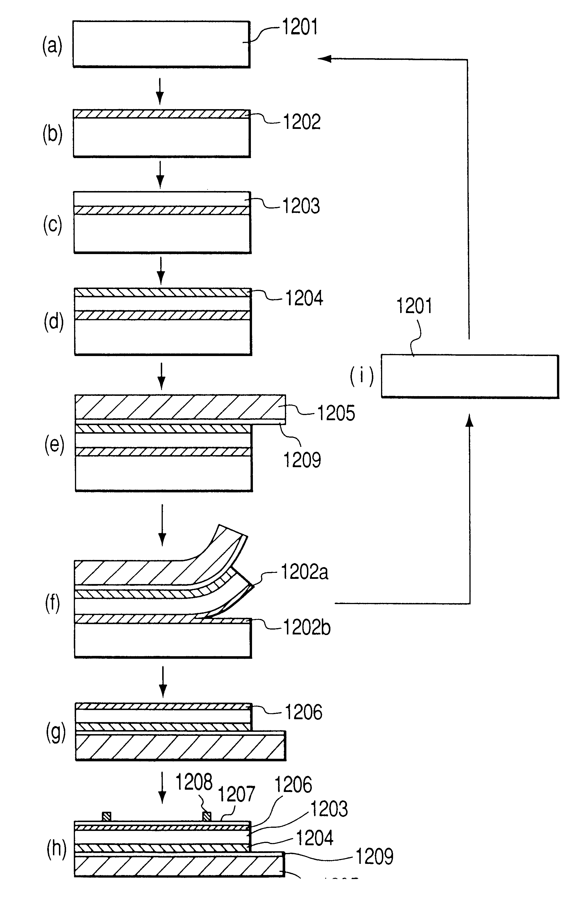
Then an adhesive film (peeling tape No. BT-315 supplied by Nitto Denko Co., Ltd.) was applied to the surface of the monocrystalline Si, then the rear face of the substrate was fixed to a vacuum chuck, and the adhesive film was then peeled off from ...

example 3

The surface layer of a monocrystalline Si wafer substrate was anodized in HF solution, under the following conditions:

current density: 7 (mA / cm.sup.2)

anodizing bath: HF:H.sub.2 O:C.sub.2 H.sub.5 OH=1:1:1

time: 4 minutes

porous Si thickness: 4.5 .mu.m

followed by:

current density: 30 (mA / cm.sup.2)

anodizing bath: HF:H.sub.2 O:C.sub.2 H.sub.5 OH=1:1:1

time: 1 minute

porous Si thickness: about 4 .mu.m

Under these conditions, there was formed a porous Si layer with two-layer structure of different porosities. In this anodizing with the current density of 30 mA / cm.sup.2, there was formed a structurally fragile porous Si layer with larger porosity.

Then the substrate was oxidized for 1 hour at 400.degree. C. in oxygen atmosphere, whereby the internal wall of the pores in the porous Si layer was covered with a thermal oxidation film. Then, on the porous Si, a monocrystalline Si was epitaxially grown, with a thickness of 0.15 .mu.m, by CVD (chemical vapor deposition) under the following conditions:

s...

example 4

In the surface layer of a monocrystalline Si substrate with an unspecified resistivity, a high concentration P.sup.+ layer of a thickness of 5 .mu.m, constituting the high concentration impurity layer, was formed by a diffusion process. At the same time a high concentration P.sup.+ layer was formed also on the back surface. Then anodizing was conducted in HF solution from the top surface side of the high concentration layer, under the following conditions:

current density: 7 (mA / cm.sup.2)

anodizing bath: HF:H.sub.2 O:C.sub.2 H.sub.5 OH=1:1:1

time: 11 minutes

porous Si thickness: 12 .mu.m

The resulting porous Si layer had a two-layer structure, with the lower porous Si having a finer and fragile structure in comparison with the surface layer part.

Then the substrate was oxidized for 1 hour at 400.degree. C. in oxygen atmosphere, whereby the internal wall of the pores in the porous Si layer was covered with a thermal oxidation film. Then, on the porous Si, a monocrystalline Si was epitaxial...


PUM


Abstract

A process for producing a semiconductor article is provided which comprises the steps of bonding a film onto a substrate having a porous semiconductor layer, and separating the film from the substrate at the porous semiconductor layer by applying a force to the film in a peeling direction.

Description

1. Field of the InventionThis invention relates-to a process for producing a semiconductor article that can suitably be used for producing a semiconductor device such as a semiconductor integrated circuit, a solar cell, a semiconductor laser device or a light emitting diode. More particularly, it relates to a process for producing a semiconductor article including a step of separating a substrate.2. Related Background ArtSemiconductor articles are popular in terms of semiconductor wafers, semiconductor substrates and various semiconductor devices and include those adapted for producing semiconductor devices by utilizing the semiconductor region thereof and those used as preforms for producing semiconductor devices.Some semiconductor articles of the type under consideration comprise a semiconductor layer arranged on an insulator.The technology of forming a single crystal silicon semiconductor layer on an insulator is referred to as silicon on insulator (SOI) technology, which is wide...

Claims


Application Information

Patent Timeline
IPC IPC(8): B28D5/00H01L21/20H01L21/66H01L21/02H01L21/18H01L21/304H01L31/06H01L31/068H01L31/18G02F1/13G02F1/1362
CPCB28D5/00H01L21/187H01L21/2007H01L21/304H01L21/76254H01L21/76259H01L22/00H01L31/068H01L31/1804H01L31/1892G02F1/136277H01L2924/0002H01L2221/68363H01L2221/68368Y02E10/547H01L2924/00Y02P70/50H01L21/02
Inventor SAKAGUCHI, KIYOFUMIYONEHARA, TAKAONISHIDA, SHOJIYAMAGATA, KENJI
Owner CANON KK
Why Eureka
Try Eureka