Process for making electronic devices having a monolayer diffusion barrier

a technology of diffusion barrier and electronic device, which is applied in the direction of semiconductor devices, semiconductor/solid-state device details, electrical apparatus, etc., can solve the problems of ic element size having two detrimental effects on the resulting ic, limited electrical conductivity of aluminum and tungsten, and reducing the resistance characteristics of the resistor, etc., to achieve the effect of increasing the versatility of the invention, and reducing the resistance characteristics

Inactive Publication Date: 2005-04-19
THE UNITED STATES OF AMERICA AS REPRESENTED BY THE SECRETARY OF THE NAVY
View PDF71 Cites 8 Cited by
  • Summary
  • Abstract
  • Description
  • Claims
  • Application Information

AI Technical Summary

Benefits of technology

[0021]Another advantage of the present invention, is that the heteroepitaxial barrier film conforms well to the surface contour of a substrate, whether the surface contour is very smooth or uneven, without leaving bare (uncoated) spots on the substrate surface, which increases the versatility of the invention. That is, the diffusion barrier layer of this invention can be implemented on not only semiconductor and electro-optic materials that have two-dimensional single crystalline surfaces, but it also has wider applicability encompassing substrate surfaces that contain crystalline defects (e.g., pits, crystalline mis-orientations, and steps). Further, the diffusion barrier layer also blocks the diffusion pathways on imperfect crystalline surfaces, and hence will be of more practical and immediate applicability with imperfect wafer surfaces, and hence the existing wafer technology. Also, in the case bulk metal halide crystals, the metal can be deposited directly on the crystal and processed according to this invention.
[0022]An important advantage of this invention is that a copper conductor can be formed on a very thin, yet effective, diffusion barrier film as a highly organized, single crystal (monocrystalline) structure. The single crystal morphology of the deposited copper yields even lower resistivity characteristics, as compared to polycrystalline forms of the metal, permitting even thinner interconnect lines. Consequently, the copper lines formed by this invention provide superior conductivity characteristics, permitting further line size reductions.
[0023]Furthermore, as the thickness of polycrystalline metal film gets smaller (e.g. on the order of approximately 400 Å or less), there is a general increase in its resistivity. This is because the conducting electrons are now scattered by the boundaries of the metal film. This is alleviated in the present invention by providing the metal film in a single crystalline morphology, in which case the electrons are scattered specularly at the surface. That is, even if the electrons are scattered, their energy and momentum are conserved because of the near-perfect atomic arrangement of the single crystalline film surface created by the present invention. Hence there is only minimal increase in the resistivity of the metal with a decrease in film thickness. Various other objects, details and advantages of the invention will be apparent from the following detailed description when read in conjunction with the drawings.

Problems solved by technology

However, because the electrical conductivity of aluminum and tungsten is limited, the lines and plugs must be made thick enough to ensure minimal resistance to electric current between components and between levels.
The relative large size of these conductors has become an issue for IC designers and fabricators interested in placing a greater density of circuit elements on an IC.
This reduction in IC element size has two detrimental effects on the resulting IC.
First, it increases the resistance of the metal interconnects.
Second, it increases the aspect ratio of the via holes, making them more difficult to fill with the metallic material.
Incomplete filling of the via holes exacerbates the problem of high resistance.
Today, there is often not enough space in the lateral direction on an IC chip to accommodate large aluminum conductors.
Additionally, the size of the via holes, when filled with tungsten, limits the number of levels in the IC.
However, a practical copper interconnect strategy for semiconductor devices has faced several problems.
For instance, copper is susceptible to corrosion because it does not form a native self protective oxide surface film.
Also, the electrochemical activity of copper is conducive to corrosion.
However, as an even more notable problem of current interest, copper has a tendency to diffuse relatively easily at elevated temperatures into silicon.
The copper which migrates into the silicon tends to produce deep-level defects, which can severely degrade the electrical characteristics of the devices.
The probability of this problem arising is heightened due to the fact that ICs must be annealed several times during the fabrication process.
That is, as known, copper is relatively difficult to etch so its implementation in interconnect schemes generally requires additive patterning, such as damascene patterning, in lieu of subtractive processing.
A thick barrier layer can frustrate the advantage of using copper interconnects.
Another practical problem associated with implementing copper interconnects arises from the present state-of-the art wafer technology.
This requirement typically is not completely met, i.e., it is not generally satisfied for the entire surface area of a standard 3 inch (7.6 cm) silicon wafer.
In addition, the crystal orientation of the wafer generally is not perfect, as consequently there will be mis-oriented grains and grain boundaries that extend to the surface of the wafer.
These imperfections on the wafer will tend to undermine conventional atomic diffusion barriers as they provide pathways for the diffusion of the copper atoms.
The problem of diffusion exists not only in the case of copper metallization on silicon, but also in the case of copper metallization on other single- and polycrystalline semiconductor substrate materials such as gallium arsenide, silicon carbide, germanium, and so forth.
Also, copper diffusion or drift into insulating or dielectric materials, such as SiO2, can result in short circuits, especially in dense arrays of IC components.
Diffusion is also a problem with other high conductivity metallization materials such as gold, silver, and platinum.

Method used


Image

  • Process for making electronic devices having a monolayer diffusion barrier
  • Process for making electronic devices having a monolayer diffusion barrier
  • Process for making electronic devices having a monolayer diffusion barrier

Examples


example 1

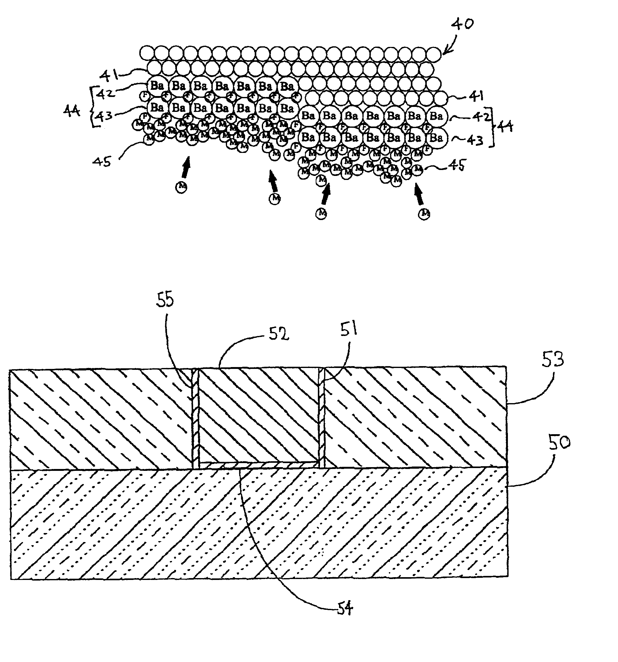
[0057]A barium / barium fluoride (Ba / BaF2) composite barrier film was grown on a silicon (100) wafer using molecular beam epitaxy (MBE), followed by formation of a single crystal metallic (elemental) copper layer on the metal halide (surface) portion of the barrier film. The films were grown inside a commercial MBE deposition chamber made by Vacuum Generators (model VG Semnicon V80H). The MBE system above has both Knudsen cells and e-beam sources for the barium fluoride, and a separate e-beam source inside the chamber for the copper, and a 30 kV RHEED system to monitor the film structure during film deposition. The substrate heater is capable of holding up to 3 inch (7.6 cm) diameter wafers and control the substrate temperature to within ±0.1° C. at 1000° C. and a maximum deviation of the temperature across the substrate of ±0.1° C. All temperature measurements are made from a noncontact thermocouple gauge, namely, an optical pyrometer having an accuracy of ±0.5° C.

[0058]A silicon (10...

example 2

[0068]A barium / barium fluoride (Ba / BaF2) composite barrier film also was grown on a single crystal gallium arsenide (001) wafer using molecular beam epitaxy (MBE), followed by formation of a single crystal metallic (elemental) copper layer on the metal halide (surface) portion of the barrier film.

[0069]To accomplish this, first, a barium fluoride film was deposited on the gallium arsenide substrate using the basic procedure described in U.S. Pat. No. 5,932,006 (see Example 1 therein) except that the (100) oriented single crystal GaAs substrate was replaced by a (001) oriented single crystal GaAs substrate for this example, which teachings are incorporated herein by reference.

[0070]Then, the procedure to grow a single crystal copper film on the BaF2 on gallium arsenide was conducted as follows. Once the barium fluoride deposition was completed the substrate temperature was lowered to 400° C. With a substrate temperature of 400° C., copper was deposited on the barium fluoride surface ...


PUM

PropertyMeasurementUnit
pressureaaaaaaaaaa
temperatureaaaaaaaaaa

Abstract

An epitaxial barrier material provides not only a unique growth medium for growing single crystal structures of elemental metal thereon, but also provides an effective diffusion barrier at extremely thin thicknesses against migration of atoms from the metallization layer into an adjacent semiconductor substrate or low dielectric insulation layer. This invention is particularly advantageous for forming single crystal, transition metal conductor lines, contacts, filled trenches, and/or via plugs, and especially conductor structures based on transition metals of copper, silver, gold, or platinum. These metals are highly attractive for interconnect strategies on account of there respective low resistivity and high reliability characteristics. Processes for making the barrier film in a semiconductor device are also covered. The capability to use copper interconnect strategies coupled with the proviso of an extremely thin barrier film makes possible a significant increase in the component density and a corresponding reduction in the number of layers in large scale integrated circuits, as well as improved performance.

Description

[0001]This is a Divisional of application Ser. No. 09 / 563,740, filed May 3, 2000, now U.S. Pat. No. 6,465,887.STATEMENT OF GOVERNMENT INTEREST[0002]The invention described herein may be manufactured and used by or for the Government of the United States of America for Governmental purposes without the payment of any royalties thereon or therefor.BACKGROUND OF THE INVENTION[0003]This invention relates generally to the fabrication of semiconductor devices, and particularly to an advanced barrier film useful for forming single crystal metal in electronic devices.[0004]Integrated circuits (ICs) are composed of vast number of active components such as transistors, resistors, and capacitors, and other active devices. These individual components are generally laid out in a two dimensional array on a substrate, such as silicon or gallium arsenide. The two dimensional arrays are often stacked on top of one another to form a three dimensional IC. As in any circuit, these components, and the s...

Claims


Application Information

Patent Timeline
Patent Type & Authority Patents(United States)
IPC IPC(8): H01L21/285H01L21/70H01L23/52H01L23/532H01L21/02H01L21/768
CPCH01L21/28518H01L21/28562H01L21/28568H01L21/76843H01L21/76846H01L21/76864H01L21/76877H01L23/53238H01L2924/0002H01L2924/00
Inventor CHU, TAK KINSANTIAGO, FRANCISCOBOULAIS, KEVIN A.
Owner THE UNITED STATES OF AMERICA AS REPRESENTED BY THE SECRETARY OF THE NAVY
Why Eureka
Try Eureka